SKEMA RANGKAIAN AMPLIFIER

MELAYANI PERBAIKAN TV DAN PERANGKAT ELEKTRONIK LAINNYA. ALAMAT JL.RAYA KARANG KEMIRI RT 01/RW 06 PURWOKERTO TELP. 082329735432

Tuesday, June 14, 2011

Flashing Batteres Monitor with 3 Led Indikator


Flashing Batteres Circuit

 
Description. Here is a simple circuit in which an LED will continue flashing as long as
the voltage of the battery to be monitored is above the set level.The transistors Q1 and
Q2 are wired as a complementary astable multivibrator.The circuit can operate from a
voltage range from 6V to 12V. The voltage level at which LED has to stop flashing can be
set by adjusting the preset R4.When the battery voltage reaches the threshold the
flashing frequency decreases and when the voltage goes below the threshold the LED
becomes OFF.The diode D1 is used to compensate the changes in the base emitter voltage
of Q1 due to temperature changes. Circuit diagram with Parts list. Notes. Assemble the
circuit on a general purpose PCB. Batteries from 6V to 12V can be monitored by this
circuit. The diode D1 must be a Schottky diode.
Read more: http://www.circuitstoday.com/category/battery-related#ixzz1PCfjcIQ0

3 Led Batteres Monitor

  
Description. This is the circuit diagram of a 3 LED bar graph type battery monitor
circuit that is ideal for monitoring the voltage level of an automobile battery.When
battery voltage is 11.5V or less transistor Q1 will be On and the LED D1 will be
glowing.When battery voltage is between 11.5 and 13.5V, the transistor Q2 will be On and
the LED D2 will be glowing.When battery voltage is above 13.5V the transistor Q3 will be
On and the LED D3 will be glowing. Circuit diagram with Parts list. Notes. Assemble the
circuit on a general purpose PCB. The battery to be monitored can be connected between
the terminals namely A and B. It is always better to use LEDs of different colour.

Read more: http://www.circuitstoday.com/category/battery-related#ixzz1PCgjWlRR

Driver Lampu Neon 8 watt dan Indikator Led Panggilan Masuk

Driver Lampu Neon 8 watt

Here is the schematic of a simple flouroscent lamp driver circuit based on two transistors.The circuit uses capacitive ballasting for driving the tube.An 8 W  standard flouroscent tube can be efficiently driven using the circuit.
The two  transistors (2Sc 1983)  with associated components forms a oscillator  around
1KHz.The oscillator is wired so that  saturation condition of the transistors are 
prohibited.This  adds on to the efficiency of the circuit.The circuit produces a clean
sine wave with very less noise.
Circuit diagram with Parts list.
Notes.
Use a 12 V battery as the DC voltage source.
Use a 8W florescent lamp as load.
The winding details(no of turns) are given in the circuit.Use  0.8 mm dia enameled
copper wire for primary and 0.4 mm dia enameled copper wire for secondary.The core can
be a ferrite core.The primary should be wound first and secondary on top of it.

Read more: http://www.circuitstoday.com/8w-flouroscent-lamp-driver#ixzz1PBFqzXxV

Kode Kunci Satu Transistor

One transistor code lock
 
This is of course the simplest electronic code lock circuit one can make. The circuit uses one transistor, a relay and few passive components. The simplicity does not have any influence on the performance and this circuit works really fine.
The circuit is nothing but a simple transistor switch with a relay at its collector as load. Five switches (S0 to S4) arranged in series with the current limiting resistor R2 is connected across the base of the transistor and positive supply rail. Another five switches (S5 to S9) arranged in parallel is connected across the base of the transistor and ground. The transistor Q1 will be ON and relay will be activated only if all the switches S0 to S4 are ON and S5 to S9 are OFF. Arrange these switches in a shuffled manner on the panel and that it. The relay will be ON only if the switches S0 to S9 are either OFF or ON in the correct combination. The device to be controlled using the lock circuit can be connected through the relay terminals. Transformer T1, bridge D1, capacitor C1 forms the power supply section of the circuit. Diode D2 is a freewheeling diode. Resistor R1 ensures that the transistor Q1 is OFF when there is no connection between its base and positive supply rail.Circuit diagram.
Notes.
This circuit can be assembled on a Vero board.
Switch S1 is the lock’s power switch.
The no of switches can be increased to make it hard to guess the combination.
Transistor 2N2222 is not very critical here. Any low or medium power NPN transistor will do the job.

Read more: http://www.circuitstoday.com/one-transistor-code-lock#ixzz1PA2yxZbN


Tv Remote Jammer
  
Here is the circuit diagram of simple but highly effective TV remote jammer circuit.
Most of the TV remotes have 38KHz operating frequency. A flood of IR beams in the same
frequency can easily confuse the TV receiver and this is the operating principle of our
jammer. The circuit is nothing but an astable multivibrator based on NE555 IC. The
output of NE555 is amplified using a PNP transistor SK100 to drive the IR LEDs. Not only
TV remotes, but any IR remotes operating in the 38KHz frequency region can be also
jammed by using this circuit.Circuit diagram.
Notes.
The circuit can be assembled on a Vero board.
Use a 9V PP3 battery for powering the circuit.
Mount the IC on a holder.
POT R4 can be adjusted to exactly match the jammer’s frequency to the remotes frequency.
This adjustment is very essential for effective jamming.

Read more: http://www.circuitstoday.com/tv-remote-jammer#ixzz1PB4sofv5

Monday, June 13, 2011

Rangkaian Subwoofer dan Port USB

Subwoofer Filter Circuit Using Op-Amp TL072
 
Here is a simple subwoofer filter circuit that can be powered by a 12V DC. This circuit
is very useful in automotive applications subwoofer. The circuit is a low pass filter
whose pass frequency can be set between 60 to 160 Hz
Subwoofer Filter Circuit Using Op-Amp TL072
Op-Amp TL072
The circuit is built around the TL072 dual op amp IC BIFET. Of the two operational
amplifiers inside the chip, IC1A is wired as a buffer. The left and right audio inputs
after mixing is fed to the input of the IC1A using the DPDT switch S1. Switch S1 is the
phase control switch which can be used to make the subwoofer in phase with other
speakers. When S1 is in position 2, 180 degree phase shift will be induced.POT R7 can be
used for controlling the level. IC1B forms the low pass filter whose pass frequency can
be controlled by adjusting the dual gang POT R13.
Note:
The circuit can be powered from 12V DC.
C5 and C6 must be polyester capacitors.
POT R13 can be used for adjusting the pass frequency.
POT R7 can be used for adjusting the level.


Source   skema-amplifier.blogspot.com


12 volt DC Power Supply from USB port


The circuit given below infact is a 5 volt to 12 volt converter. It uses the 5 Volts
from USB port and converts it to 12 volts DC with the help of IC LT1618.
Description :
Using this circuit we can convert 5V DC from the computer USB port to 12V DC and a
circuit like this will find a lot of application in USB powered systems. The heart of
this circuit is IC LT1618 which is a constant current, constant voltage boost converter.
The IC has a wide input voltage range of 1.8 to 18V DC and output voltage can be up to 35V DC.
In the circuit resistors R1, R2 sets the output voltage. Pin number 9 is the shutdown
pin, less than 0.3V to this pin will shut down the IC. Pin number four is the current
sense adjust pin. The current sense voltage can be reduced by applying a DC voltage to
this pin. If this adjustment is not needed connect this pin to ground and you can omit
components R3, R5 and Q1.
Circuit diagram of 12 volts dc power supply:
Circuit Diagram-12Volts DC power supply from USB port
Notes :
C2 and C3 must be rated at least 15V.
Less than 0.3V at the shutdown pin will shutdown the IC.
Output voltage is governed by the following equation R1 = R2 (  (Vout /1.263V) -1).

Read more: http://www.circuitstoday.com/12v-from-usb-port#ixzz1P9sMcj2v

Power Supply Kamera Digital

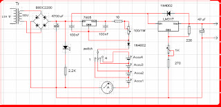
DIGITAL CAMERA PSU AND BATTERIES CHARGER

 
This ambit was created for agenda cameras. It's accepted the agenda cameras accept ample
ability consumption. For archetype my camera Minolta E223 requires about 800 mA. In
convenance a mains ability accumulation or aerial accommodation NiMH accumulators
(batteries) can amuse this demand.
This ambit consists of two parts, charger and adapter. The transformer, rectifier arch
and absorber condensator are common. Adapter is absolutely artlessly its capital
allotment is an adjustable voltage regulator LM 317 according to accepted setting.
Output is a acceptable for camera jack plug. Voltage can be adapted in ambit 2-9 V.
In the charger ambit a 7805 anchored voltage regulator works as accepted architect
assured connected accepted during charging. This charging accepted can be adapted with
the 100 /1W potentiometer in ambit about 50-300 mA adumbrated by a baby accepted
barometer instrument. From one to four batteries can be answerable simultaneously. The
about-face charge be set according to cardinal of batteries, and charging accepted of
batteries accustomed by architect charge be adjusted. This ambit doesn't admeasurement
charging time and charging action of batteries. Manufacturers accord charging time,
usually 14-16 h. I apparent this botheration with a simply, bargain automated mains
timer. I anticipate its accurateness is sufficient.
Source   skema-amplifier.blogspot.com

25Watt Audio Amplifier Mosfet

25Watt Audio Amplifier Mosfet IRF530-IRF9530


The following is a circuit of 25Watt High Quality power amplifier Mosfet IRF530-IRF9530
from Motorola's transistors are employed in the preceding stages. The supply rails
prudentially voltage was kept at the rather low value of + and - 32V.
Skema Rangkaian 25Watt Audio Amplifier Mosfet
Note:
Q6 & Q7 must have a small U-shaped heatsink.
Q8 & Q9 must be mounted on heatsink.
Adjust R11 to set quiescent current at 100mA (best measured with an Avo-meter connected
in series to Q8 Drain) with no input signal.
A correct grounding is very important to eliminate hum and ground loops. Connect to the
same point the ground sides of R1, R4, R9, C3 to C8. Connect C11 to output ground. Then
connect separately the input and output grounds to power supply ground.
List Component

R1,R4_________47K 1/4W Resistors
R2____________4K7 1/4W Resistor
R3____________1K5 1/4W Resistor
R5__________390R 1/4W Resistor
R6__________470R 1/4W Resistor
R7___________33K 1/4W Resistor
R8__________150K 1/4W Resistor
R9___________15K 1/4W Resistor
R10__________27R 1/4W Resistor
R11_________500R 1/2W Trimmer Cermet
R12,R13,R16__10R 1/4W Resistors
R14,R15_____220R 1/4W Resistors
R17___________8R2 2W Resistor
R18____________R22 4W Resistor (wirewound)
C1___________470nF 63V Polyester Capacitor
C2___________330pF 63V Polystyrene Capacitor
C3,C5________470µF 63V Electrolytic Capacitors
C4,C6,C8,C11_100nF 63V Polyester Capacitors
C7___________100µF 25V Electrolytic Capacitor
C9____________10pF 63V Polystyrene Capacitor
C10____________1µF 63V Polyester Capacitor
Q1-Q5______BC560C 45V 100mA Low noise High gain PNP Transistors
Q6_________BD140 80V 1.5A PNP Transistor
Q7_________BD139 80V 1.5A NPN Transistor
Q8_________IRF530 100V 14A N-Channel Hexfet Transistor
Q9_________IRF9530 100V 12A P-Channel Hexfet Transistor

sumber   skema-amplifier.blogspot.com

Sunday, June 12, 2011

Mini Amplifier IC LM380

Mini Amplifier IC LM380
Based amplifier IC's offer many advantages including high efficiency, high gain, low standby current, low component count, small size and, of course, low cost. It is little wonder that audio amp IC's have replaced most discrete transistors in consumer electronic devices. While many experimenters have stayed away from these little black Mysteries, I am going to uncover some of their secrets and demonstrate how easy they are to use
Rangkaian Amplifier IC LM380

Amplifier IC LM380 comes in two flavors; LM380 and LM380-8 with output powers of 700 milli-watts and 2 watts respectively. A schematic drawing below depicts the 8th and LM380-LM380.
The LM380-8 comes in an 8-pin package and its basic circuit is virtually identical to the LM380 except for the different pin out. The LM380 comes in a 14-pin package and pins 3,4,5,10,11 and 13 are connected to ground to act as a heat sink. Experience has shown the LM380 should be soldered directly to the circuit board (no IC socket) if it is going to be operated at its full rated output of 2 watts. This IC can become quite warm and it's important to get rid of excess heat through the pins. The primary advantages of the LM380 series IC's are higher output power, very low distortion and low external parts count.
Source  skema-amplifier.blogspot.com

Game Baru Tomb Raider


Game Anyar Tomb Raider Dirilis 2012


    Download Gamenya DiSini...[]

Seri terbaru Tomb Raider akan dirilis 2012
LOS ANGELES - Pengembang game Crystal Dynamics berencana meluncurkan seri terbaru instalemen game populer Tomb Raider pada 2012 mendatang.Pengumuman itu disampaikan Crystal Dynamics pada perhelatan Electronic Entertainment Expo (E3) 2011 yang dimulai Selasa waktu setempat di Los Angeles Convention Center.
Belum diketahui apa judul yang akan disematkan pada instalemen terbaru Tomb Raider
tersebut. Namun trailer dan sejumlah cuplikan gameplay-nya sudah dipamerkan pihak
pengembang pada pameran tersebut.Pada seri terbaru ini, tokoh utama Lara Croft tampil sebagai wanita 21 tahun yang baru lulus kuliah dan haus akan petualangan. Jiwa petualangan Lara akhirnya membawa dirinya terdampar di pulau misterius dengan penghuni pulau yang membahayakan.
Menurut Head of Studio Crystal Dynamics Darrell Gallagher, seri ini menceritakan petualangan Lara Croft sebelum menjadi tokoh jagoan wanita yang dikenal para gamer seluruh dunia.
"Perjalanan tersebut akan menentukan karakter Lara di masa mendatang. Game ini
menceritakan bagaimana dia menemukan jati dirinya dan berhasil menjadi prajurit tangguh
setelah melewati petualangan tersebut," jelas Gallagher seperti dikutip Bit Tech, Rabu (8/6/2011).
Rencananya game terbaru Tomb Raider baru akan rilis pada musim gugur 2012.
(van). source   okezone.com

100 watt Amplifier for Car

100W Quad Car Amplifier


 This quad ?nal amplifier is actually intended to be used in a car, but it can naturally also be used for a variety of other medium-power applications. The TDA7375A can be successfully used in all situations in which a reasonable amount of audio power is desired and only a relatively low supply voltage is available. This IC is the successor to the TDA7374B, which forms the heart of the active loudspeaker system described earlier this year. Such a quad IC amplifier is naturally an excellent choice for this application, especially since the individual amplifiers can be connected in pairs in the bridge con?guration, which allows them to provide approximately four times as much power.The new IC can handle a peak voltage of 50 V (10 V more than the TDA7374B), but what is more important is that it is also truly intended to be used for single-ended operation. It includes all imaginable types of protection in order to avoid the premature demise of the four amplifiers, and in fact it is ideally suitable for a ‘no-nonsense’ mini surround-sound system. For more information about the TDA7375A, we refer you to its data sheet, which can be found at www.st.com. The circuit shown here has four trimpots for individually setting the output levels of the amplifiers.

In addition, all inputs have RC networks (R1/C1, etc.) to block possible RF interference. The function of R6 is to separate the grounds of the input and output stages, in order to avoid possible ground loops that might arise with the use of multiple modules. A 5-W type is used for this resistor, in order to prevent it from going up in smoke if the ground connection of the power supply comes loose. C10 decouples the internal voltage divider, which biases the internal amplifier stages to half of the supply voltage. RC network R5/C9 provides a delayed, plop-free switch-on.

C15 and C16 are local bypass capacitors for the supply voltage. The power supply ripple rejection of the TDA7375A is approximately 50 dB. If you want to use only a transformer, bridge rectifier and smoothing capacitor for the power supply, the minimum requirement is a transformer rated at 12 V / 30 VA in combination with a 10,000-µF electrolytic capacitor (remember that the maximum allowable supply voltage is 18 V). One of the few drawbacks of this quad ampli?er is that two of the channels are inverted with respect to the other two. For this reason, the polarity of each loudspeaker terminal is marked on the circuit board layout (e.g., +LS1 and –LS4) to indicate which terminal of the loudspeaker should be connected where.

Radial electrolytic capacitors rated at 3300µF/16V and having a diameter of only 12 mm are used for the output capacitors, which allows the circuit board to remain relatively compact. Our preferred type of electrolytic capacitor is a member of the Rubycon ZL series, which can handle no less than 3.4 A of ripple current. The maximum current consumption of the circuit with all four channels driven to the clipping level (with 4-? loads) is approximately 2.1 A. The TDA7375A can also be used with 2-? loads. However, in this case the internal temperature rises considerably, since the Multiwatt 15V package has a rather large thermal impedance of 1.8 ºC/W.

In the interest of the service life of the IC, it is thus a good idea to use a somewhat larger heat sink. A 4 A/T fuse has been selected in consideration of possible 2-? operation. If you limit the load to 4 ?, the fuse value can be reduced to 2 A/T. The output terminals of the ampli?ers can be found on the circuit board next to the associated electrolytic capacitors. The related ground connections for LS1 and LS2 are located next to the LS1 and LS2 terminals, but the ground connections for LS3 and LS4 are located on the left, next to the IC, since this gives the best current paths on the circuit board and the least distortion. Vertical car connectors (spade terminals) are used for the power supply connections.

Resistors:
R1-R4 = 100?
R5 = 10k?
R6 = 0?1, 5W
P1-P4 = 10 k preset
Capacitors:
C1,C3,C5,C7 = 15nF
C2,C4,C6,C8 = 220nF
C9 = 10µF 63V radial
C10 = 47µF 25V radial
C11-C14 = 3300µF 16V
C15 = 100nF
C16 = 1000µF 25V radial, max. diameter 13mm
Semiconductors:
IC1 = TDA7375A (ST)
Miscellaneous:
F1 = fuse, 4A/T (time lag), with PCB mount holder 2 fast-on (spade) terminal, male, vertical, solder type (2-pin version)
Measurement results
Supply voltage = 14.4 V
Quiescent current = 100 mA
Pmax. (0.1% THD) = 4 x 5.3 W/ 4?
Input sensitivity = (5.2 W/4 ?) 0.5 V
THD+N (B = 80 kHz, 1 kHz 1W/4 ?) = < 0.04 % Bandwidth = 28 Hz to 55 kHz
source   extremecircuit.net

50W Audio Amplifier Using TDA1562

50W Audio Amplifier Using TDA1562

The integrated output amplifier described in this article consists of little more than one integrated circuit. It is intended especially for use in motor vehicles and other battery-operated applications. Although it appears simple and hardly worth looking at, the amplifier can produce an appreciable audio power output. The circuit diagram in Figure 2 emphasizes how few external components are needed to construct a complete output amplifier.
For instance, the new device does not need compensation networks to enhance the stability. Also, because of the absence of switch-on phenomena, there is no need for a switch-on delay network. There is, of course, still a need for supply line decoupling capacitors. Capacitors C5 and C6 are required for Class-H operation, about which more in the box. The value of input capacitors C1 and C2 is relatively low, thanks to the high input impedance of the IC. Switched RC network R4-C4 at the ‘mode select’ input (pin 4) serves to switch the IC to ‘mute’ or ‘standby’.
When the supply voltage is switched on, the IC is first switched automatically to the ‘mute’ mode and to ‘on’ only after a short delay. The time constant R4-C4 is a few tenths of a second and this delay between the two states is sufficient to obviate disturbing (and annoying) switch-on phenomena. Switch S1 enables the amplifier to be switched to ‘standby' when the use of the amplifier is not needed for a period of time. When that time has elapsed, the amplifier is quickly reverted to normal operation. The current drain in the standby mode is virtually negligible at only 200µA. Resistor R3 prevents a short-circuit current ensuing when S1 is being closed at the instant C4 is being discharged.
Measurement results (at Ub=14.4 V)
Supply voltage
8–18 V
Sensitivity
760 mV r.m.s.
Input impedance
70 k?
Power output
54 W r.m.s. into 4 ? (f=1 kHz; THD+N=1%)
Harmonic distortion (THD+N)
at 1 W into 4 ?: 0.046% (1 kHz)
0.29% (20 kHz)
at 35 W into 4 ?: 0.12% (1 kHz)
0.7% (20 kHz)
Signal-to-noise ratio (with 1 W into 4 ?)
88 dBA
Power bandwidth
7.5 Hz – 185 kHz (at 25 W into 4 ?)
Quiescent current
about 135 mA (‘on’)
Resistors:
R1 = 1M?
R2 = 4k?7
R3 = 1k?
R4 = 100k?
Capacitors:
C1,C2 = 470nF
C3,C4 = 10µF 63V radial
C5,C6,C8 = 4700µF 25V radial
(18mm max. dia., raster 7.5 mm)
C7 = 100nF, raster 5 mm
Semiconductors:
D1 = high-efficiency-LED
IC1 = TDA1562Q (Philips)
Miscellaneous:
S1 = single-pole on/off switch
Four spade connectors, PCB mount Heatsink for IC1 (Rth<2.5 K/W)
sumber  extremecircuit.net

Rangkaian Infrared Cordless Headphone Amplifier

Rangkaian Infrared Cordless Headphone Amplifier

Using this low cost Project one can reproduce AUDIO from TV without disturbing anyone. It does not use any wire between TV and HEADPHONE. In place of pair of wires it uses invisible Infrared light to transmit audio signals from TV to Headphone. Without using any lens a range of up to 6 meters is possible. Range can be extended by using Lenses and Reflectors with IR sensors comprising transmitters and receivers. IR transmitter uses two-stage transistor amplifier to drive two IR leds connected in series. An audio output transformer is used (in reverse) to couple Audio output from TV to the IR transmitter.
source   skema-amplifier.blogspot.com

Saturday, June 11, 2011

Rangkaian USB Sound Card

Rangkaian USB Sound Card PCM2702

The core of this construction is 16-Bit Stereo Digital-To-Analog Convertor with USB interface PCM2702.
PCM2702 needs only few additional parts to work. The schematic is not complex. Sound card can be powered directly from USB port (jumper W1) or from external power supply (jumper W3). PCM2702 needs two power supply 3.3V (3V-3.6V) and 5V (4.5V-5.5V). I used fixed output voltage LDO TPS76733Q for 3.3V (IO2) and adjustable output voltage LDO TPS76701Q for 5V (IO3). Both LDO are produced by TI, I used this because I had it in my drawer. Any similar LDO can be used. Output voltage of IO3 should be set to little bit lower than input voltage to allow LDO good stabilization, in my case output voltage is set to 4.8V. Output voltage can be set by adjustable resistor R33. In case of low power supply, IO3 can be shorted by jumper W3. LED D3 signalizes power on.
Small ferrite beads are placed before all power pins of PCM2702 and in Vbus and GND of USB. These small beads reduce high frequency hum. I had a problem find this small SMD ferrite beads in local stores but finally I acquire few of them from old hard drive. They are not absolutely necessary, you can use zero ohm resistors instead of them.
Low-pass filter is placed in output signal path to reduce sampling frequency. An OPA2353UA dual op amp is configured as a stereo 2nd-order low-pass filter. Led diode D1 is illuminated when PCM2702 plays audio data received from the USB bus. Led diode D2 is illuminated when USB bus suspends audio data transmission to the PCM2702.


IC 4069 Alternating On-Off Switch Circuit

 
Get the circuit instead of a standard on-off switch. Switching is very gentle. If we don’t use the PCB, connect unused input pins to an appropriate logic level (’+’ or ‘-’). Unused output pins *NEED* be left open!
On the Print Circuit Board this has completed already . One step ’push’ activates the relay, another ‘push’ de-activates the relay.
IC1 (the 4069) is a regular Hex-inverter type and is constructed with MOS P-channel and N-channel
enhancement mode devices in a single monolithic structure.
Accessories List

R1 = 10K
R2 = 100K
R3 = 10K
R4 = 220 Ohm (optional)
C1 = 0.1µF, Ceramic (100nF)
C2 = 1µF/16V, Electrolytic
D1 = 1N4001
Led1 = Led, 3mm, red (optional)
Q1 = 2N4401 (see text) IC1 = 4069, CMOS, Hex Inverter (MC14069UB), or equivalent
S1 = Momentary on-switch
Ry1 = Relay )
Description of circuit.
It is going to operate on voltages from 3 to 18 volts, but most applications are in the 5-15 volts. Although the IC1 4069 contains protection circuitry against damage from ESD , use common sense when handling this device. Depending on your application you may want to use an IC-socket with IC1. It makes replacement easy if the IC ever fails. The IC is CMOS so watch for static discharge! You can use any type of 1/4 watt resistors including the metal-film type.
The type for D1 in not critical, even a 1N4148 will work. But, depending on your application I would suggest a 1N4001 as a minimum if your relay type is 0.5A or more. Any one in the 1N400x series diodes will work.
Any proper replacement for Q1 will work, including the european TUN’s. Since Q1 is just a driver to switch the relay
coil, almost any type for the transistor will do. PN100, NTE123AP, BC547, 2N3904, 2N2222, 2N4013, etc. will all work for the relays mentioned here. For heavier relays you may need to change Q1 for the appropriate type.
For C2, if you find the relay acts not fast enough, you can change it to a lower value. It is there as a spark-arrestor together with diode D1.
For the relay I used an 8 volt type with the above circuit and a 9 volt battery. Depending on your application, if the current-draw is little, you can use a cheap 5V reed-relay type. Use a 8V or 9V relay type if your supply voltage is12V. Or re-calculate resistor R3 for a higher value.
The circuit and 9V will work fine and will pull the relay between 7 and 9 volt, the only thing to watch for is the
working voltage of C2; increase that to 50V if you use a 12V supply.
The pcb was designed for an Aromat/Omron relay, 12V/5A, #HB1-DC12V. You can easily re-design the relay pads on the PCB for the relay of your choice. If you wish to use something you already have, and you don’t want to re-design the PCB, you can glue the relay up-side-down on the pcb and wire the relay contacts manually to the pcb-holes or directly to your application. Use a 2N2222 transistor for Q1 if your supply voltage is higher than 9V and/or your relay is heavy duty, or doesn’t want to pull-in for any other reason.
Again, the pcb drawing is not to scale. Use ‘page-setup’ to put the scale to 103% for a single pcb, vertically, and your scale should be correct. I use a laser printer and so I don’t know if this scale of 103% is for all printers. Tocheck, print a copy onto regular paper and see if the IC pins fit the print. If so, your copy is correct. If not,
change the scale up of down until a hardcopy fits the IC perfectly.
The Led is nice for a visual circuit indication of being ‘on’. For use with 12V supply try making make R4 about 330ohms. The LED and R4 are of course optional and can be omitted. Your application may already have some sort ofindicator and so the LED and R4 are not needed.
sumber   skema-rangkaian-elektronika.blogspot.com

SKEMA RANGKAIAN UPS MINI

SKEMA RANGKAIAN UPS MINI


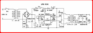
UPS (Uninterruptible Power Supply), is used to anticipate the power off. Despite UPS
Reliable not the original, this series of little means, merakitnnya How do I ...?
Simple and easy. The cost is relatively cheaper to buy rather than the original UPS.
What about the components that are required? Many sold in electronic stores. Thus you
will be losers if they do not try merakitnya.
Output series UPS has a power of 1.5 W. Before the main series of the withdrawal there
is a series of mini adapter that has a voltage between 9V/12V with strong currents of
500mA. Voltage generated is used to operate the series and fill the battery. UPS is
designed to keep electronic devices can run even if the electricity off.
How to Work??
When the inverter is run with the AC input, and a change in DC voltage. At the output
penyearah used to fill the battery. When the power fails or the electric current
extinction occurs, flow to the dc voltage inverter, which then generate the output AC
voltage inverter (more details, see picture).
series of connected around the CD4047 IC multivibrator that operates at a frequency of
50 Hz. Multivibrator Q output of this drive MOSFETs IRF540. Outout inverter direduksi
and filtered using a MOV (Metal Oxide Vasitor). Tranformer used is 9-0-9, 1.5A. Two LED
(d6 and D7) is used as an indicator whether the main voltage or baattery that are
working.
UPS (Uninterruptible Power Supply), is used to anticipate the power off. Despite UPS
sehandal not the original, this series of little means, merakitnnya How do I ...?
Simple and easy. The cost is relatively cheaper to buy rather than the original UPS.
What about the components that are required? Many sold in electronic stores. Thus you
will be losers if they do not try merakitnya.
Output series UPS has a power of 1.5 W. Before the main series of the withdrawal there
is a series of mini adapter that has a voltage between 9V/12V with strong currents of
500mA. Voltage generated is used to operate the series and fill the battery. UPS is
designed to keep electronic devices can run even if the electricity off.
How to Work Series
When the inverter is run with the AC input, and a change in DC voltage. At the output
penyearah used to fill the battery. When the power fails or the electric current
extinction occurs, flow to the dc voltage inverter, which then generate the output AC
voltage inverter (more details, see picture).
series of connected around the CD4047 IC multivibrator that operates at a frequency of
50 Hz. Multivibrator Q output of this drive MOSFETs IRF540. Outout inverter direduksi
and filtered using a MOV (Metal Oxide Vasitor). Tranformer used is 9-0-9, 1.5A. Two LED
(d6 and D7) is used as an indicator whether the main voltage or baattery that are working.


INVERTER WITH IC 555


Series of DC-AC inverter produces AC output voltage as voltage net. IC 555 configured as a low frequency oscillator. Frequency can be changed from 50 to 60 Hz with a frequency potensio meter change R4.
This DC-to-AC inverter schematic produces an AC output at line frequency and voltage. The 555 is configured as a low-frequency oscillator, tunable over the frequency range of 50 to 60 Hz by Frequency potentiometer R4.
The 555 feeds its output (amplified by Q1 and Q2) to the input of transformer T1, a reverse-connected filament transformer with the necessary step-up turns ratio. Capacitor C4 and coil L1 filter the input to T1, assuring that it is effectively a sine wave. Adjust the value of T1 to your voltage.
The output (in watts) is up to you by selecting different components.
Input voltage is anywhere from +5V to +15Volt DC, adjust the 2700uF cap's working voltage accordingly.
Replacement types for Q1 are: TIP41B, TIP41C, NTE196, ECG196, etc. Replacement types for Q2 are: TIP42B, TIP42C, NTE197, ECG197, etc. Don't be afraid to use another type of similar specs, it's only a transistor... ;-)
Parts List:

R1 = 10K
R2 = 100K
R3 = 100 ohm
R4 = 50K potmeter, Linear
C1,C2 = 0.1uF
C3 = 0.01uF
C4 = 2700uF
Q1 = TIP41A, NPN, or equivalent
Q2 = TIP42A, PNP, or equivalent
L1 = 1uH
T1 = Filament transformer, your choice
If the whole thing is working, good. If not, relax and don't get frustrated. Do the following checks:
1. You have connected the filament transformer in REVERSE yes?
2. If not, disconnect the power and reverse. If you have, disconnect the transformer and measure the voltage after L1 and ground.
3. Just in case, GROUND for this circuit is same as negative (-).
4. Q1/Q2 are oposites, e.i. npn/pnp.
5. Is your 555 perhaps defective? Disconnect R3 from pin 3 and check pin 3 for a pulse.
6. Check your transistors to make sure they are not defective.

Error fix: Pin 7 and 2 were reversed. Original pinout was correct.
source  skema-rangkaian-elektronika.blogspot.com

Sound Effect

 Skema Sound Effect

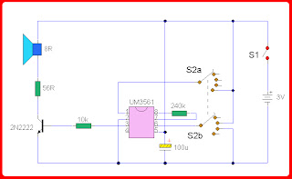
This circuit uses a UM3561 IC to produce four different sound effects.
UM3561 IC Sound Effect Generator Circuit
                               Notes
Nothing too complicated here. The IC produces all the sound effects, the output at Pin 3
being amplified by the transistor. A 64 ohm loudspeaker can be substituted in place of
the 56 ohm resistor and 8 ohm loudspeaker. The 2 pole 4 way switch controls the sound
effects. Position 1 (as drawn) being a Police siren, position 2 is a fire engine sound,
3 is an ambulance and position 4 is a machine gun effect. The IC is manufactured by UMC
and was available from Maplin electronics code UJ45Y. At the time of writing this has
now been discontinued, but they have have limited stocks available.
UM3561 Availability
The IC sound generator UM3561 is now available in a kt from Maplin Electronics. Click
here for the link. Special thanks to Shaibul Alom for pointing this out to me.


SKEMA RANGKAIAN EQUALIZER 5 BAND
 
In this part of the investigation in a series of 5-band Equalizer circuits with a single IC BA3812 namely L, a device used in the hi-fi.IC BA 3812 This is L IC with 5-point Equalizer with all the functions integrated in one IC. To get a clear picture of the circuit is a series of pictures, click on it.
To Equalizer has advantages, namely: small distortion, a small noise, dinamic local area, and is suitable for a series of hi-fi stereo. And with a wide voltage range from 3.5 volt to 16 volt.voltage is the recommended 8 volt but according in market 9volt highest voltage and 16 volt adl.
sumber  skema-rangkaian-elektronika.blogspot.com

Protektor Speaker


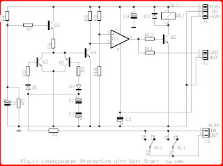
This series also has advantages, namely: the case of consleting relationship with the
speaker amplifier series will be lost directly, so that the speaker's safe fire.time to
waiting or delay time is about 5 seconds, and can be changed with the change elco
condenser C2 to the value of smaller . The time needed to open the relay back when the
flow be around 0.5 seconds. Or you can try using a series of under this scheme:
R1=22Kohm C4-5=100uF 25V IC1=TL071
R2-3=390Kohm Q1=BC560C RL1=Relay 12VDc Omron G2R2
R4=470Kohm Q2-3-4=BC550C J1=3pin connector with 2.54mm step
R5=1Mohm Q5=BD139 J2=2pin connector with 2.54mm step
R6-7-8-9-10-12=10Kohm D1-2-3=1N4148 J3=2pin connector with 3.96mm step
R11=820 ohm D4=Green 5mm Led
C1-2-3=47uF 63V D5=Red 5mm Led
source  skema-rangkaian-elektronika.blogspot.com


RF Remote Control 2 Channel

RF Remote Control 2 Channel

Receiver SchemeThe receiver constituted by RF receiver bore RLP434A at 418MHz, the microcontroller
AT90S2313 and the 2 relays with can handle any electric (or electronic) accessory up to
10 Amps (the contacts of my relays are 10Amp at 250Volts).
The RLP434A is an RF receiver bore with cancellation abundance at 418MHz with ASK
modulation. There are 2 outputs from this module, the digital, with levels from 0v to
VCC (5 volts in our case) and the analog output. Analog achievement is not used. The
transmitter accelerate 4 bytes with 2400bps 4 times and the receiver RLP-434A, aggregate
them and move them to AT90S2313 to RxD pin, PD0.
Two affidavit to baddest AT90S2313 (20pins) instead of AT90S2343 (8pins) is because
a.) AT90S2313 use a accouterments UART adapted at 2400bps and the accouterments UART is
added stable, with abate code, than software UART that I use in the transmitter. If some
consecutive abstracts access at the middle-time of some added accepted added than accept
routine, for abiding we will apart this $.25 of data. The accouterments UART does not
accept this botheration because accept absorber for this (UDR register). This is what I
beggarly that the accouterments UART is "stable".
b.) with AT90S2313 we can drive up to 14 relays with approaching advancement of the
firmware, one broadcast to anniversary pin.
As antenna you can use a cable 30 - 35cm long
RF Remote Control 2 Channel Transmitter Scheme
The transmitter is constituted by AT90S2323 microcontroller and TLP434 RF transmitter
bore at 418MHz. I accept designe the transmitter for added array abridgement and safe
transmition of the data.
* The array abridgement is fabricated it by the use of powerdown approach of AVR. In
this case the AVR goes to beddy-bye with beneath than 1uA (microampere) accepted and
delay for alien arrest on pin PB1 to alive from beddy-bye and abide operating.
If you columnist the S2 key, the argumentation of this pin goes to '0' (0V) and AVR
alive frome the beddy-bye approach (because PB1 is INT0) and analysis if apprenticed the
S1 key. If not, the AVR booty as apprenticed key the S2. If yes the AVR booty as
apprenticed key the S1.
If you columnist the S1 key the argumentation of this pin and PB1 (through 1N4148) goes
to '0' (0V). In this case the AVR booty as apprenticed key the S1.
After, account the checksum and address 4 times the aforementioned 4 byte arrangement to
accomplish abiding that receiver takes the abstracts and goes to beddy-bye approach
until abutting arrest on PB1.
When the INT0 pin (PB1) of AVR goes to 0V, the transmitter TLP434A is working. If you
stop columnist the about-face S1 or S2, the TLP is stop working.
* The safe transmition of the abstracts based to transmition of 4 bytes with consecutive
anatomy at 2400 bps (bits per seconds). 1st and 2nd byte are for acceptance of accurate
alien ascendancy from receiver (like ID bytes), 3rd byte is command byte. The relays
cachet dependet by the amount of this byte. Finaly, the 4th byte is the checksum of the
beforehand 3 bytes.
example: if byte1=30h, byte2=35h and byte3=02h the 4th byte (chechsum) will be (byte1)
XOR (byte2) XOR (byte3) = 30h XOR 35h XOR 03h = 06h.
This adjustment use 4 bytes x 8 bit anniversary = 32 bit breadth (without alpha and stop
bits). That is beggarly 1 achievability at 4.294.967.295 to accept the receiver, the
aforementioned 4 bytes from some added RF device.
This transmitter will assignment with all 2323 chips but bigger is AT90LS2323 with alive
voltage 2.7 - 6 volts.The microcontroller that I use is AT90S2323 with alive voltage 4 -
6 volts. Its formed accomplished with 3v lithium battery.
As antenna you can use ~7cm cable in to transmitter`s box.
source  skema-rangkaian-elektronika.blogspot.com


Rangkaian Wireless Microphone

Komponen Rangkaian Wireless Microphone

R1 = 10K (brown-black-orange)
R2,R3 = 100K (brown-black-yellow)
R4 = 470 ohm (yellow-violet-brown)
C1,C3 = 4.7pF (4p7), ceramic
C2,C4 = 4.7uF-16V, electrolytic
C5 = 0.001uF (1nF), ceramic
C6 = 470pF, ceramic
Q1,Q2 = 2N2222, NPN transistor
L1 = 1uH, variable inductor
Mic = Electret mike, 2 wires
Couple Notes:
Q1 amplifies the input signal via C4 from the electret microphone.
Q2 acts as an oscillator and the signal coming off C2 is fed onto the base of Q2.
L1/C1 is a so called ‘tank’ circuit and operates in the 88-105MHz band on your regular
AM/FM radio dial.
L1 is a 1uH variable inductor coil to be able to tune it a little bit, and the range of
1uH is approximate.
The antenna can be as simple as a 8″ (21cm) piece of wire of any kind.
source  skema-rangkaian-elektronika.blogspot.com


Skema Rangkaian Penerima TV

Skema Rangkaian Penerima TV

A VHF band TV transmitter using negative sound modulation and PAL video modulation. This
is suitable for countries using TV systems B and G.
Notes:
The frequency of the transmitter lies within VHF and VLF range on the TV channel,
however this circuit has not been tested at UHF frequencies. The modulated sound signal
contains 5.5 -6MHz by tuning C5. Sound modulation is FM and is compatible with UK System
I sound. The transmitter however is working at VHF frequencies between 54 and 216MHz and
therefore compatible only with countries using Pal System B and Pal System G.
source  skema-rangkaian-elektronika.blogspot.com


Friday, June 10, 2011

Software Pembaca Nilai Resistor


Seperti yang sudah dibahas dalam posting tentang resistor sebelumnya di artikel Cara membaca nilai resistor, kemampuan membaca resistor wajib diketahui oleh rekan rekan teknisi, terlebih itu teknisi repair / service, boleh dikatakan semua perangkat elektronika dari radio usang sampai komputer semuanya menggunakan komponen dasar resistor.
Untuk yang sudah terbiasa dengan dunia teknik elektronika tentunya membaca nilai sebuah resistor itu sama sekali bukan masalah. Pada intinya kita hanya perlu mengetahui angka2 standar yang dimiliki oleh resistor, misalnya 1,1.0,2,2.2 dst..dan nilai dari warna cincin terakhir sebagai faktor pengali, bagi yang sudah terbiasa dilihat sekilas pun sudah ketahuan resistansinya.
Tetapi bagi yang masih awam dengan resistor ini tentunya kesulitan membaca hambatan sebuah resistor, perlu waktu belajar. Kebetulan saat ini sudah ada sofware untuk membaca nilai sebuah resistor secara cepat, ini juga bisa digunakan oleh anda yang ingin praktis langsung mengetahui resistansi resistor. Sebenarnya dari dulu software ini sudah ada, hanya saja fiturnya belum lengkap, resistor yang bisa dibaca hanya yang memiliki 4 cincin saja.
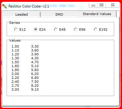
Sedangkan untuk software versi terbaru yaitu Resistor Color Coder v2.1 sudah bisa membaca nilai resistor dengan 5 cincin warna. Dilengkapi juga dengan Pembacaan Resistor SMD, yang resistansinya menggunakan sistem angka. Misalnya 473 berarti 47Kohm atau 272 yang berarti 2,7Kohm. Fitur tambahan lainnya yaitu sejenis panduan untuk berapa saja angka angka resistor standar itu, saya pernah membahas nya dulu di Variasi nilai hambatan pada Resistor.
Untuk lebih jelasnya silahkan lihat screenshot Software Pembaca Nilai Resistor dibawah ini :

Untuk membaca nilai resistor sebelumnya anda harus memilih terlebih dahulu jenis resistor tersebut, bisa metal film / resistor dengan 1% atau resistor standar yang memiliki toleransi 5% opsi ini terlihat di sebelah kanan software yang ditandai dengan gambar resistor. Untuk selanjutnya tinggal klik klik warna yang bersangkutan dan nilai resistor pun akan tampil dengan sendirinya.


Ini merupakan tampilan untuk membaca resistansi resistor jenis SMD yang biasa digunakan pada resistor, tinggal masukkan saja angka yang tertera pada badan resistor dan nilai dari resistor akan tampil, mudah bukan….


Tampilan yang terakhir ini merupakan fitur baru juga, fungsinya untuk mengetahui berapa saja nilai standar pada resistor itu, seperti bisa dilihat pada screenshot diatas angka angkanya yaitu 1 – 3.3 – 3.6 dst….
Jika anda ingin mendownload software ini bisa langsung ke http://www.schematica.com/ dan pilihlah download sofware resistor.
referensi : http://www.infoservicetv.com

Rangkaian Tone Kontrol

Mono Tone Kontrol


Tone kontrol mono atau tunggal adalah tone kontrol yang hanya mempunyai satu input sinyal dan satu output sinyal suara.


Stereo Tone Kontrol


Sebenarnya stereo tone kontrol adalah gabunga dari dua buah mono tone kontrol.


Amplifier Sanken


This is a  power amplifier blazer circuit provides up to 1000Watt . This interesting routes many good bass and treble alive. Importantly should choose Power supply source, which has been fairly high voltage class 70Vdc GND -70V 10A is the current low level
The transistors 2SC3858 and 2SA1494 are feature high bandwidth, excellent safe operating area, high linearity and high gain. Driver transistors are 2SC5200 and 2SA1943. All devices are rated at 230V, with the power transistors having a 150W dissipation and the drivers are 50W.
1000 watt Blazer Amplifier Circuit
This circuit describes an amplifier, power supply and tests procedures that are all inherently dangerous. Nothing described in this article should even be considered unless you are fully experienced, know exactly what you are doing, and are willing to take full 100% responsibility for what you do. There are aspects of the design that may require analysis, fault-finding and/or modification.
source skema-amplifier.blogspot.com

Stereo Amplifier Class A

 20 Watt Class A Amplifier

he amplifier circuit uses the basic circuitry of the 70W power amplifier, but modified
for true Class-A operation - it should be pretty nice! This amp has been built by
several readers, and the reports I have received have been very positive.
With simulations, everything appears to be as expected, but although I have yet to
actually build it and test it out thoroughly, no-one has had any problems so far. Using +/-20 Volt supplies - either conventional, regulated or using a capacitance multiplier, it should actually be capable of about 22 W before clipping, but expect to use a big
heatsink - this amp will run hot.l.)Rangkaian 20 Watt Class-A Power Amplifier
The current sink shown should have very high linearity, since it is based on the same
concept as the output stage devices. The 0.25 Ohm resistor should cause little grief (4
x 1 Ohm 1W resistors in parallel), but some experimentation may be needed here, since
the base-emitter voltage of the BC549 determines the current. This circuit works by
using the BC549 to steal any excess base current from the compound pair. As soon as the
voltage across the 0.25 Ohm resistor exceeds 0.65V, the transistor turns on and achieves
balance virtually instantly.The 1k trimpot in the collector of the first LTP transistor allows the DC offset to be
adjusted. The nominal value is around 400 ohms, but making it variable allows you to set
the output DC offset to within a few mV of zero.


 1000 Watt Power Amplifier


his is a scheme set 1000watt power amplifier. Currently I do not have a picture to the circuit board, but because the amplifier circuit is quite simple, you can design it
yourself PCB easily. Or you can order it at the store PCB audio kit in the center of electronic singosaren oriental, solo.the assemble cables for DC power supply and output transistors must be large, use size
1.5-3mm for large current passed. The supply used transformer with 20A/45Ct and at least
4x10000uf/80 volt capasitor. this circuit is able to supply power 10000watt therefore
the power transistor will be very hot, give good cooling fan on the power transisitor
Transitor alternative to replacement of the 2SA1494 is 2SA1216 From SANKEN. The
transistor has a 200-350 watt power dissipation of each pair so that for long-term
operation of more durable. Keep in mind, usually sold a pair of power transistors with
its complement, so you can not buy 2SC2922 alone without 2SA1216 or 2SA1494 without
2SC3858. The price range for transitor tsb is 30-40 thousand Rupiah / pair.

sumber skema-amplifier.blogspot.com

Thursday, June 9, 2011

Stereo Amplifier TDA

120 Watt Stereo Amplifier
 
Here is a 120 watt stereo amplifier circuit using STK4241V. The MAX9710 a stereo audio power amplifier IC capable of delivering 2 x 120 Watts of out put to 8 Ohm loads. MAX9710 can be operated from a single ±32V to ±54V power supply.
120 Watt Stereo Amplifier Circuit Using IC STK4241V ,STK4241V IC
This amplifier circuit is suitable for home power audio devices. The STK4241V amplifier specifications might lead you to believe that it can use supply voltages of up to ±78V. With zero input signal (and therefore no output) it might, but I don't recommend anything greater than ±45V if 8 ohm loads are expected, although ±54V will be fine if you can provide good heatsinking.


 10 Watt Amplifier

This audio amplifier Circuit is a class-B audio power amplifier using a TDA1010. It is easy to construct and has only a few external components. The circuit is designed with short circuit and thermal protection. It can drive loads as low as 1.6 ohm and is capable of deliveringover 10 watts from a 16 V DC power supply.
Skema Rangkaian 10W Audio Amplifier TDA1010
The TDA1010 is a monolithic integrated class-B audio amplifier circuit in a 9-lead single in-line (SIL) plastic package. The wide supply voltage range and the flexibility of the IC make it an attractive proposition for record players and tape recorders with output powers up to 10 W.

Sumber skema-amplifier.blogspot.com

Skema Rangkaian Elektro


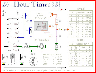
Kedua sirkuit yang multi-range timer menawarkan jangka waktu sampai 24 jam dan seterusnya. Keduanya pada dasarnya sama. Perbedaan utama adalah bahwa ketika waktu habis, Versi 1 energi pada relay dan Versi 2 de-memberikan energi itu. Yang pertama menggunakan daya yang lebih kecil, sementara timer sedang berjalan, dan yang kedua menggunakan daya yang lebih kecil setelah timer berhenti. Pilih satu yang paling sesuai dengan aplikasi Anda.
The Cmos 4060 adalah counter biner 14 bit dengan built in osilator. Osilator ini terdiri dari dua inverter terhubung ke Pins 9, 10 & 11; dan frekuensi diatur oleh R3, R4 & berkedip C3.The Led hijau sedangkan osilator berjalan: dan IC menghitung jumlah osilasi. Meskipun sedikit 14 counter, tidak semua bit dapat diakses. Mereka yang dapat dicapai akan ditampilkan pada gambar.

 Audio Ampifier Khusus Untuk Gitar


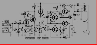
This is a circuit of an audio amplifier for the guitar. This circuit can reproduce a Combo amplifier of the type very common in the 'Sixties and the' Seventies of the past century. It is well suited as a guitar amplifier but it will do a good job with any kind of electronic musical instrument or microphone.
5W power output was a common feature of these widespread devices due to the general adoption of a class A single-tube output stage (see the Vox AC-4 model). Furthermore, nowadays we can do without the old-fashioned streetcars VIB-feature frequently included in those designs.Read More...


Most battery chargers cannot be left connected to the battery for long periods of time as over-charging and consequent battery damage will occur. This add-on circuit is placed in series with the battery being charged and is powered by the battery itself. In effect, the circuit uses a high-current Mosfet to control the charging current and it turns off when the battery voltage reaches a preset threshold. Power for the circuit is fed from the battery to 3-terminal regulator REG1 which provides 8V .Read More...

Jam Digital


Kedua sirkuit yang multi-range timer menawarkan jangka waktu sampai 24 jam dan seterusnya. Keduanya pada dasarnya sama. Perbedaan utama adalah bahwa ketika waktu habis, Versi 1 energi pada relay dan Versi 2 de-memberikan energi itu. Yang pertama menggunakan daya yang lebih kecil, sementara timer sedang berjalan, dan yang kedua menggunakan daya yang lebih kecil setelah timer berhenti. Pilih satu yang paling sesuai dengan aplikasi Anda.
The Cmos 4060 adalah counter biner 14 bit dengan built in osilator. Osilator ini terdiri dari dua inverter terhubung ke Pins 9, 10 & 11; dan frekuensi diatur oleh R3, R4 & berkedip C3.The Led hijau sedangkan osilator berjalan: dan IC menghitung jumlah osilasi. Meskipun sedikit 14 counter, tidak semua bit dapat diakses. Mereka yang dapat dicapai akan ditampilkan pada gambar.

Dengan menyesuaikan frekuensi osilator, Anda dapat mengatur durasi waktu yang dibutuhkan untuk setiap output yang diberikan untuk pergi tinggi. Output ini kemudian beralih transistor, yang pada gilirannya beroperasi estafet. Pada saat yang sama, D1 berhenti hitungan dengan menonaktifkan osilator. Idealnya harus C3 non-terpolarisasi; tetapi biasa elektrolitik akan bekerja, asalkan tidak bocor terlalu buruk di arah sebaliknya. Atau, Anda dapat mensimulasikan 10uF non-terpolarisasi kapasitor dengan menghubungkan dua 22uF kapasitor kembali ke belakang (seperti yang ditunjukkan).

Menggunakan "Trial and Error" untuk menetapkan jangka waktu yang lama akan sangat membosankan. Solusi yang lebih baik adalah dengan menggunakan tabel Setup yang disediakan, dan menghitung waktu yang dibutuhkan untuk Pin 7 untuk pergi tinggi. Setup tabel pada kedua skema yang dipertukarkan. Mereka hanya dua cara yang berbeda untuk mengekspresikan persamaan yang sama.

Misalnya, jika Anda ingin jangka waktu 9 Jam, Range tabel menunjukkan bahwa Anda bisa menggunakan output pada Pin 2. Anda perlu Pin 2 untuk pergi tinggi setelah 9 x 60 x 60 = 32 400 detik. Tabel Setup memberitahu Anda untuk membagi ini dengan 512; memberikan sekitar 63 detik. Sesuaikan R4 sehingga Kuning lampu LED 63 detik setelah power diterapkan. Hal ini akan memberikan output pada Pin 2 setelah sekitar 9 jam.
Timer ini dirancang untuk persediaan 12-volt. Namun, memberikan relay yang cocok digunakan, rangkaian akan bekerja di apapun dari 5 sampai 15-volt. Menerapkan daya mulai timer. Tersebut dapat direset setiap saat dengan gangguan singkat catu daya. Tombol reset adalah opsional, tetapi TIDAK harus digunakan selama setup. Waktu yang diperlukan untuk Kuning LED untuk cahaya HARUS diukur dari kekuatan saat diterapkan. Meskipun R1, R2 dan dua LED membantu dengan setup, mereka tidak perlu dengan operasi timer. Jika Anda ingin mengurangi konsumsi daya, lepaskan mereka setelah Anda menyelesaikan setup. Jika Anda membutuhkan waktu yang lebih lama dari 24-jam, meningkatkan nilai C3.
sumber skema-amplifier.blogspot.com

Audio Amplifier Gitar


Audio Ampifier Khusus Untuk Gitar

This is a circuit of an audio amplifier for the guitar. This circuit can reproduce a Combo amplifier of the type very common in the 'Sixties and the' Seventies of the past century. It is well suited as a guitar amplifier but it will do a good job with any kind of electronic musical instrument or microphone.
5W power output was a common feature of these widespread devices due to the general adoption of a class A single-tube output stage (see the Vox AC-4 model). Furthermore, nowadays we can do without the old-fashioned streetcars VIB-feature frequently included in those designs.
Skema Rangkaian Audio Ampifier Khusus Untuk Gitar
List Component Of Gitar Ampifier

P1______________4K7 Linear Potentiometer
P2_____________10K Log. Potentiometer

R1,R2__________68K 1/4W Resistors
R3____________220K 1/4W Resistor
R4,R6,R11_______4K7 1/4W Resistors
R5_____________27K 1/4W Resistor
R7______________1K 1/4W Resistor
R8______________3K3 1/2W Resistor
R9______________2K 1/2W Trimmer Cermet
R10___________470R 1/4W Resistor
R12_____________1K5 1/4W Resistor
R13___________470K 1/4W Resistor
R14____________33K 1/4W Resistor

C1____________100pF 63V Ceramic Capacitor
C2____________100nF 63V Polyester Capacitor
C3____________470µF 35V Electrolytic Capacitor
C4____________220nF 63V Polyester Capacitor (Optional, see Notes)
C5_____________47µF 25V Electrolytic Capacitor (Optional, see Notes)
C6______________1µF 63V Polyester Capacitor
C7,C8,C9,C10___47µF 25V Electrolytic Capacitors
C11____________47pF 63V Ceramic Capacitor
C12__________1000µF 35V Electrolytic Capacitor
C13__________2200µF 35V Electrolytic Capacitor

D1_____________5mm. Red LED
D2,D3________1N4004 400V 1A Diodes

Q1,Q2________2N3819 General-purpose N-Channel FETs
Q3____________BC182 50V 200mA NPN Transistor
Q4____________BD135 45V 1.5A NPN Transistor (See Notes)
Q5____________BDX53A 60V 8A NPN Darlington Transistor
Q6____________BDX54A 60V 8A PNP Darlington Transistor

J1,J2________6.3mm. Mono Jack sockets

SW1____________1 pole 3 ways rotary switch (Optional, see Notes)
SW2____________SPST Mains switch

F1_____________1.6A Fuse with socket

T1_____________220V Primary, 48V Center-tapped Secondary
20 to 30VA Mains transformer

PL1____________Male Mains plug

SPKR___________One or more speakers wired in series or in parallel
Total resulting impedance: 8 or 4 Ohm
Minimum power handling: 20W

The present circuit can deliver 10W of output power when driving an 8 Ohm load, or about 18W @ 4 Ohm.It also features a two-FET Preamplifier, two inputs with different sensitivity, a treble-cut control and an optional switch allowing powerful overdrive or treble-enhancement.
sumber skema-amplifier.blogspot.com

Charger Otomatis


Most battery chargers cannot be left connected to the battery for long periods of time as over-charging and consequent battery damage will occur. This add-on circuit is placed in series with the battery being charged and is powered by the battery itself. In effect, the circuit uses a high-current Mosfet to control the charging current and it turns off when the battery voltage reaches a preset threshold. Power for the circuit is fed from the battery to 3-terminal regulator REG1 which provides 8V.

Rangkaian Automatic 12V Battery Charger

LED1 indicates that the battery is connected and that power is available. The 555 timer IC is configured as an astable oscillator running at approximately 100kHz. It feeds a diode pump (D1 & D2) to generate adequate gate voltage for Mosfet Q3, enabling it to turn on with very little on resistance (typically 14 milliohms). With the Mosfet turned on, current flows from the charger's positive terminal so that charging can proceed. The battery voltage is monitored by 10kO pot VR1.

When the wiper voltage exceeds the conduction voltage of zener diode ZD1, transistor Q1 turns on and pulls pin 4 (reset) low to switch off the 555 and remove gate drive to the Mosfet. This process is progressive so that the cycle rapidly repeats itself as the battery charges. Eventually, a point is reached when the battery approaches its charged condition and the cycle slows right down. Transistor Q2 and LED2 function as a cycle indicator. When the battery is under charge, LED2 appears to be constantly on. When the battery is fully charged, LED2 briefly flicks off (charging) and returns to the on state (not charging) for a longer period.

Source http://www.extremecircuits.net.

Power Supply Variable


Power supply with variable voltage and fixed current regulation made using the ubiquitous L200C regulator. The versatile 5 pin L200C regulator offers both voltage and current regulation in a single package. The IC also features thermal shutdown and input over voltage protection up to 60 Vdc. The package is also available as L200CV which has straight pins for mounting onto a PCB.

Skema Rangkaian L200 Variable Power supply

The above circuit has current limiting of 1 amp, hence Rsc = 0.45 ohm. The output voltage is variable from 2.85V to 36V. For voltages up to 36V then the input voltage, Vcc must be 40V. The supply voltage must always a few volts higher than the maximum output voltage. If you wanted to make a 9 Volt current limited PSU then the input voltage should be a minimum of 12 Volts.
L200 Pinout

L200 Chip Specifications:
DC Input Voltage: 40V max.
Peak Input Voltage: 60V max. for 10ms
Output Voltage Range: 2.85 to 36V
Output Current Range: 0.1 to 2A
Quiescent Current: 4.2mA
Output Noise: 80uV

This variable power supply circuit from www.zen22142.zen.co.uk

Volume Kontrol Stereo Digital


An array of well-matched resistors and a low noise active output stage that is capable of driving a 600 Ohm load is included in this device. Through 95.5 dB attenuation and 31.5 dB of gain , a total adjustable range of 127 dB, in 0.5 dB steps, is achieved.
Daisy-chaining of multiple Cs3310's for multi-channel audio system is provided by the simple 3-wire interface. This device has an input/output voltage range of +- 3.75 V and can be operated from +- 5V supplies. Refer to its datasheet or more information about how to use this device. [Source: Cirrus Logic]
Free counters!