SKEMA RANGKAIAN AMPLIFIER

MELAYANI PERBAIKAN TV DAN PERANGKAT ELEKTRONIK LAINNYA. ALAMAT JL.RAYA KARANG KEMIRI RT 01/RW 06 PURWOKERTO TELP. 082329735432

Thursday, June 30, 2011

Intercom Circuit

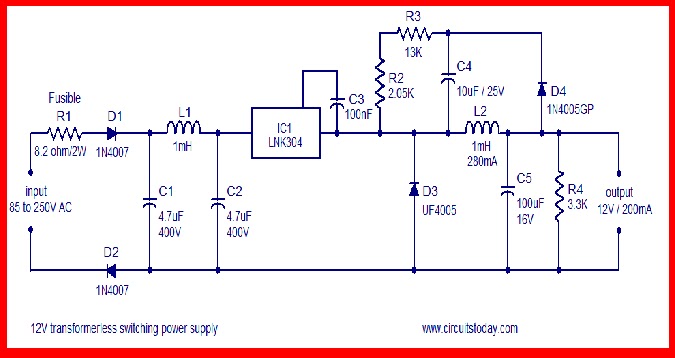
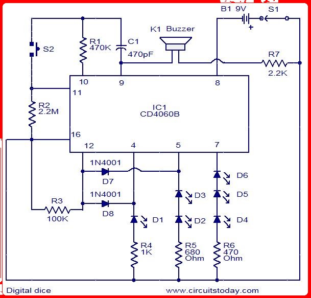
 A simple intercom circuit designed based on transistors is shown here. This intercom circuit does not require a changeover switch and you can use it just like a telephone and a ringer circuit is also included.
IC1 UM66 and transistor Q1 forms the ringer section. When pushbutton switch S1 is pressed UM66 produces a musical tone. This tone is amplified by Q1 and is coupled to the collector of Q2. Condenser Mic M1 is used to pick the conversation and Q2 is used to amplify it. R2 powers the condenser Mic while C2 is the DC decoupling capacitor for the amplifier stage based on Q2. The next stage of the circuit is a transformer coupled push pull amplifier stage based on L1, Q3 and Q4. Capacitor C5 is the power supply filter while capacitor C4 couples the output of the push pull amplifier to the ear piece. source  circuitstoday.

Water level Alarm Circuit

 Here is a simple water level alarm circuit that will produce an audible alarm when the water level reaches  a preset level.The circuit can be powered of a  3V battery and is very handy to use.

The circuit is based on an astable multivibrator wired around IC1 (NE 555).The operating frequency of the astable multivibrator here will depend on capacitor C1, resistances R1,R2 and the resistance across the probes A&B.When there is no water up to the probes,they will be open and so the multivibrator will not produce oscillations and the buzzer will not beep.When there is water up to the level of probes,some current will pass through the water,the circuit will be closed to some extend,and the IC will start producing oscillations in a frequency  proportional to the value of C1,R1,R2 and the resistance of water across the probes.The buzzer will beep to indicate the presence of water up to the level of the sensing probes.source circuitstoday.com

Stereo Decoder Circuits

Dingdong Sound Generator
This is the circuit diagram of a ding dong sound generator based on two NE555 timer ICs.The circuit is designed to toggle between two adjustable frequencies to produce the ding dong sound. The first NE555 (IC1) is wires as an astable multivibrator operating at 1Hz. The frequency of the second NE555 (IC2) is modulated by the output from the first IC. MORE...>

Power Supply 120 MA
12V/120mA switch mode power supply circuit.Transformer less switch mode power supplies have become very popular these days. The circuit shown below is of a 12V/120mA output, 85 to 230V AC input transformerless switch mode power supply using LNK304 IC. Applications of a power supply based on this IC includes hand held devices, timers, small appliances, LED drivers, industrial gadgets etc.LNK304 is a low component count, efficient off-line switcher IC that can support buck, buck-boost and flyback topologies. MORE...>
 
Stereo Decoder Circuit
In FM stereo transmission left and right channels are algebraically encoded into sum (left + right) and difference (left-right) signals. This is done in order to make the mono FM receivers compatible with the stereo transmission. The mono receiver will reproduce the summed left and right channel and the listener will hear both these channels through a single loud speaker. Stereo decoder is a circuit which is used in stereo FM receivers in order to recover the left and right channel information from the composite transmission signal. This task is achieved by adding the difference signal to the summed signal to recover left channel and subtracting the difference signal from the summed signal to recover the right channel. MORE...>

Stereo Decoder Circuit

In FM stereo transmission left and right channels are algebraically encoded into sum (left + right) and difference (left-right) signals. This is done in order to make the mono FM receivers compatible with the stereo transmission. The mono receiver will reproduce the summed left and right channel and the listener will hear both these channels through a single loud speaker. Stereo decoder is a circuit which is used in stereo FM receivers in order to recover the left and right channel information from the composite transmission signal. This task is achieved by adding the difference signal to the summed signal to recover left channel and subtracting the difference signal from the summed signal to recover the right channel.
The circuit diagram of a stereo decoder using MC1310P IC from Motorola is shown below. MC1310P is an integrated stereo decoder IC chip which is available in 14 pin DIL plastic package.
Circuit description.
In the circuit composite signal if fed to the input pin (pin2) of the IC through decoupling capacitor C12. Capacitors C6 and C7 do the job of power supply filtering. Capacitor C3 plus Resistors R3 and R4 forms the RC for the ICs internal oscillator circuit. Resistor R2 plus capacitors C1 and C2 forms a loop filter. D1 is an indicator LED and R1 limits the current through it. The decoded left and right stereo outputs are available at pins 4 and 5 respectively. C10 and C11 are the DC decoupling capacitors for the left and right outputs.

Temperatur Control DC Fan

Here is a simple circuit based on two transistors that can be used to control the speed of a 12 V DC fan depending on the temperature.A thermistor (R1) is used to sense the temperature. When the temperature increases the base current of Q1 (BC 547) increases which in turn decreases the collector voltage of the same transistor. Since the collector of Q1 is coupled to the base of Q2 (BD 140), the decrease in collector voltage of Q1 forward biases the Q2 more and so do the speed of the motor. Also, the brightness of the LED will be proportional to the speed of the motor.

Circuit diagram with Parts list.

Notes.
The R1 can be a 15K @ 20°C ,N.T.C  thermistor.
The M1 can be a 12V,700mA fan motor.
The capacitor C1 must be rated 25V.
The circuit can be powered from a 12V PP3 battery or 12V DC power supply.
Assemble the circuit on a good quality PCB or common board.

Wednesday, June 29, 2011

Power Supply 10 MA - 12 volt

12V/120mA switch mode power supply circuit.
Transformer less switch mode power supplies have become very popular these days. The circuit shown below is of a 12V/120mA output, 85 to 230V AC input transformerless switch mode power supply using LNK304 IC. Applications of a power supply based on this IC includes hand held devices, timers, small appliances, LED drivers, industrial gadgets etc.LNK304 is a low component count, efficient off-line switcher IC that can support buck, buck-boost and flyback topologies. The IC has a built in auto start circuit for short circuit and open loop fault protection. Other features of LNK304 includes low temperature variation, thermal shut down,high break down voltage, good line & load regulation, high band width , wide input voltage range (85 to 230V AC) etc. In general the LNK304 has a better performance when compared to the many other discrete buck regulators.LNK304 pin configuration and typical application
The pin configuration and the typical application diagram of LNK304 are shown above. Drain (D) pin the drain connection of the built in power MOSFET. The external by pass capacitor (0.1uF) is connected to the BYPASS (BP) terminal. FEEDBACK (FB) pin controls the switching of the built in power MOSFET. A current above than 49uA delivered to this pin will inhibit the switching. The internal power MOSFETs source is connected to the SOURCE (S) pin.
12V /120 switch mode power supply circuitThe circuit diagram of a practical 12V/120mA transformerless switch mode power supply is shown above.
Resistor R1, capacitors C1 and C2, diodes D1 and D2 and inductor L1 forms the input stage. D1 and D2 forms the rectifier section while C1 and C2 are input filters. Resistor R1 which is a fusible resistor limits the inrush current, increases differential mode noise attenuation and also serves as an input safetyfuse.The next stage is the regulator stage which consists of IC LNK304, diodes D3 and D4, capacitorsC3, C4 and C5, resistors R3, R4 and R5 and inductor L2. D3 is the freewheeling diode while L2 isthe output choke. C5 is the output filter capacitor which limits the output ripple voltage to a value as low as possible. The IC LNK304 is so configured that the power supply operated in the most discontinuous mode and that’s why a fast recovery diode (UF4005) is used as the freewheeling diode (D3). UF4005 has a reverse recovery time of around 75nS and it is well enough for the given situation.The voltage drop across diodes D3 and D4 are practically same and so the voltage across C4 tracks the output voltage and this voltage is picked by the network comprising of resistors R2, R3 and is fed to the feedback pin. R2 and R3 sets the output voltage and for 12V output the voltage at the feedback pin must be 1.65V DC. The circuit attains regulation by skipping the switching cycles. When the output voltage rise, the current at the feedback pin also rises and when the current rises above the threshold value, subsequent cycles are skipped until the current at the feedback pin goes below the
threshold and thus a constant output voltage is maintained.The IC will auto restart if no cycles are skipped during a 50mS time period and this limits the maximum output power to 6% of the maximum over load power. That’s how over load protection is attained. Resistor R4 serves as a small preload which nullifies the effects of tracking error.
source: http://www.circuitstoday.com

Tuesday, June 28, 2011

Dingdong Sound Generator

This is the circuit diagram of a ding dong sound generator based on two NE555 timer ICs.The circuitis designed to toggle between two adjustable frequencies to produce the ding dong sound. The firstNE555 (IC1) is wires as an astable multivibrator operating at 1Hz. The frequency of the second NE555(IC2) is modulated by the output from the first IC. This is attained by connecting the output of first IC to the control pin (pin5) of the second IC. The tone of the sound depends on the frequency of the second IC and the changeover time depends on the frequency of the first IC.
Notes.
The circuit can be assembled on a Vero board.
Use 9V PP3 battery for powering the circuit.
POT R4 can be used to adjust the tone of the sound.
POT R2 can be used to adjust the change over time.
IC1 and IC2 must be mounted on holders.
K1 can be a 8 ohms, 1/2 watt tweeter.
source:http://www.circuitstoday.com

Monday, June 27, 2011

Zero Crossing Detektor

Zero-crossing detector is an applied form of comparator. Either of the op-amp basic comparator
circuits discussed can be employed as the zero-crossing detector provided the reference voltage Vref
is made zero. Zero-crossing detector using inverting op-amp comparator is depicted in figure. The
output voltage waveform shown in figure indicates when and in what direction an input signal vin
crosses zero volt. In some applications the input signal may be low frequency one (i.e. input may be
a slowly changing waveform). In such a case output voltage vOUT may not switch quickly from one
saturation state to the other. Because of the noise at the input terminals of the op-amp, there may
be fluctuation in output voltage between two saturation states (+ Vsat and – Vsat voltages). Thus
zero crossings may be detected for noise voltages as well as input signal vin. Both of these problems
can be overcome, if we use regenerative or positive feeding causing the output voltage vout to change
faster and eliminating the false output transitions that may be caused due to noise at the input of
the op-amp.
source:http://www.circuitstoday.com

MNC TV
TV UNO


Sunday, June 26, 2011

Astro Tv online

Rangkaian Lampu Berdenyut


Konverter Dc 12-24 volt

The circuit diagram of a very simple voltage doubler using NE555 timer is shown here. Here IC NE555 is wired as an astable mutivibrator operating at around 9KHz. The base of the two transistors (Q1 and Q2) is shorted and output of the astable multivibrator (pin 3) is connected to it. When the output of astable multivibrator is low, Q1 will be OFF and Q2 will be ON. The negative terminal of the capacitor C3 will be shorted to ground through T2 and it will be charged to the input supply voltage. When the output of the astable multi vibrator is high, transistor Q1 will be ON and transistor Q2 will be OFF. The capacitor C4 will be charged to the voltage across capacitor C3 plus the input supply voltage (that is double the input voltage). This is how the circuit works.
This voltage doubler circuit can deliver only up to 50mA output current and above that current limit the output voltage will be dramatically reduced. The actual output voltage will be around 19V for a 12V DC input and also the output voltage will be a bit unstable. Anyway, for low current applications this circuit is well enough.

source: http://www.circuitstoday.com

Battere Eliminator Circuit

Here is the circuit diagram of a battery eliminator circuit that can be used as a
replacement for 9V PP3 batteries. The circuit given here can be used to power any device
that operates from a 9V battery. The transformer T1 steps down the mains voltage and
bridge D1 performs the job of rectification. Capacitor C1 is a filter. IC LM317T is the
regulator here. The value of R1, R2 and R3 are so selected that the output voltage of
IC1 will be steady 9 volts.
Notes.
Assemble the circuit on a good quality PCB.
Transformer T1 can be a 230V primary, 9V secondary, 1.5A step down transformer.
If 1A Bridge is not available, then make one using four 1N 4007 diodes.
Do not connect loads that consume more than 1.5A to this circuit.
A heat sink is recommended for IC1.
source: http://www.circuitstoday.com

Saturday, June 25, 2011

Convert Cdroom to Audio cd player

    Here is the simplest scheme for converting a CD ROM drive of your computer to a Audio CD
player.The minimum requirement for the player is that, it should have a audio output and
skip button. Luckily most of the Cd ROM’s are equipped with both of these.
The CD ROM drive needs two voltages ,12V & 5V for its operation.So the main objective is
to build a suitable power supply for the CD ROM drive.The IC1 (7812) together with
associated components produce a regulated 12V DC.The IC2 (7805) together with associated
components produce a regulated 5V DC.These voltages as well as ground can be connected
to the corresponding voltage pins of the CD ROM drive using a male type CD ROM drive
power connector.The 12V can be connected to the yellow wire of connector, 5V to red wire
and GND to black wire as shown in figure1.Now the power supply is ready.
Make the circuit as shown in the circuit diagram.Power up the circuit after connecting
the power connector to the CD ROM drive. Now the power LED of the drive will glow.Insert
the audio CD.Now the music will be available at the audio output socket of the drive.It
can be heared using a headphone.The skip button of the drive can be used to play next song.
By connecting the audio output to a power amplifier you can enjoy the music in a greater
wattage.Click Here! to get the amplifier circuits suitable for this project.
Notes.
For car stereo applications you don’t need the transformer,rectifier and the 7812
regulator.12V will be available from battery.You just need to produce a 5V from it using
a 7805 based regulator. Connect the corresponding voltages to the connector as shown in
figure 1 and connect the connector to drive.Done.
The amplifier for the car audio CD player must be one operating from 12V.
Do not connect the voltages to CD ROM drive in wrong polarity.Double check the voltages
using a multimeter. Wrong polarity could easily damage the drive.
source:www.circuitstoday.com

Speaker to Microphone Converter Circuit

  This circuit is a simple approach for converting a loud speaker into a microphone. When
the sound waves fall on the diaphragm of a speaker, there will be fluctuations in the
coil and there will be a small proportional induced voltage. Usually this induced
voltage is very low in magnitude and useless. Here in the circuit the low voltage is
amplified using transistors to produce a reasonable output. The transistor Q1 is wired
in common base mode and produces the required voltage gain. The transistor Q2 is wired
as an emitter follower to produce enough current gain. The voice quality of this circuit
will not be as much as a conventional microphone but quite reasonable quality can be
obtained. To set up the circuit, keep the preset R2 at around 10 Ohms and connect the
battery. Now adjust R2 to obtain the optimum sound quality.
Notes.
Assemble the circuit on a general purpose PCB.
Power the circuit from a 9 V PP3 battery.
A 3 inch speaker can be used as K1.
All capacitors must be rated at least 15V.
An 8 Ohm speaker or head phone can be connected at the output to hear the picked sound
source: http://www.circuitstoday.com

Light to Frequency Converter Circuit

    Here is the circuit diagram of a effective light to frequency converter circuit that can
be used for variety of applications such as light intensity measurement,fun etc.
The circuit is based on TLC555, the CMOS version of famous timer IC NE 555. A photo
diode is used for sensing the light intensity.The timer IC is wired in astable mode.The
leakage current of the reverse biased photo diode is proportional to the light intensity
falling on it.This leakage current charges the capacitance C1.When the capacitor voltage
reaches 2/3 of the supply voltage the out put (pin 3) goes low.As a result the capacitor
discharges through photo diode .When the capacitor voltage reaches 1/3 the supply
voltage the out put (pin 3) of IC goes high.This cycling continues and we get a
frequency at pin 3  proportional to the light intensity falling on the photo diode.
Notes.
With the given components the frequency  varies from 1KHZ @ complete darkness to  24 Khz
@  bright sunlight.The frequency range can be changed by using different values for C1.
Use any general purpose photo diode for D1
source: http://www.circuitstoday.com

Friday, June 24, 2011

Digital To Analog Konverter

 A D/A Converter is used when the binary output from a digital system is to be converted into its equivalent analog voltage or current.The binary output will be a sequence of 1's and 0's. Thus they ma be difficult to follow. But, a D/A converter help the user to interpret easily.Basically, a D/A converter have an op-amp. It can be classified into 2 types. They are
1. Digital to Analog Converter using Binary-Weighted ResistorsA D/A converter using binary-weighted resistors is shown in the figure below. In the circuit, the op-amp is connected in the inverting mode. The op-amp can also be connected in the non-inverting mode. The circuit diagram represents a 4-digit converter. Thus, the number of binary inputs is four.Digital-to-Analog Converter Circuit - Binary-Weighted Resistors MethodWe know that, a 4-bit converter will have 24 = 16 combinations of output. Thus, a corresponding 16 outputs of analog will also be present for the binary inputs.Four switches from b0 to b3 are available to simulate the binary inputs: in practice, a 4-bit binary counter such as a 7493 can also be used.
Working
The circuit is basically working as a current to voltage converter.b0 is closedIt will be connected directly  to the +5V.Thus, voltage across R = 5V
Current through R = 5V/10kohm = 0.5mA
Current through feedback resistor, Rf = 0.5mA (Since, Input bias current, IB is negligible)
Thus, output voltage = -(1kohm)*(0.5mA) = -0.5V
b1 is closed, b0 is open
R/2 will be connected to the positive supply of the +5V.
Current through R will become twice the value of current (1mA) to flow through Rf.
Thus, output voltage also doubles.
b0 and b1 are closed
Current through Rf = 1.5mA
Output voltage = -(1kohm)*(1.5mA) = -1.5V
Thus, according to the position (ON/OFF) of the switches (bo-b3), the corresponding “binary-weighted” currents will be obtained in the input resistor. The current through Rf will be the sum of these currents. This overall current is then converted to its proportional output voltage. Naturally, the output will be maximum if the switches (b0-b3) are closedV0 = -Rf *([b0/R][b1/(R/2)][b2/(R/4)][b3/(R/8)]) – where each of the inputs b3, b2, b1, and b0 may either be HIGH (+5V) or LOW (0V).The graph with the analog outputs versus possible combinations of inputs is shown below.Digital-to-Analog Converter Circuit - Binary-Weighted Resistors Method GraphThe output is a negative going staircase waveform with 15 steps of -).5V each. In practice, due to the variations in the logic HIGH voltage levels, all the steps will not have the same size. The value of the feedback resistor Rf changes the size of the steps. Thus, a desired size for a step can be obtained by connecting the appropriate feedback resistor. The only condition to look out for is that the maximum output voltage should not exceed the saturation levels of the op-amp. Metal-film resistors are more preferred for obtaining accurate outputs.DisadvantagesIf the number of inputs (>4) or combinations (>16) is more, the binary-weighted resistors may not be readily available. This is why; R and 2R method is more preferred as it requires only two sets of precision resistance values.
2. Digital to Analog Converter with R and 2R Resistors
A D/A converter with R and 2R resistors is shown in the figure below. As in the binary-weighted resistors method, the binary inputs are simulated by the switches (b0-b3), and the output is proportional to the binary inputs. Binary inputs can be either in the HIGH (+5V) or LOW (0V) state. Let b3 be the most significant bit and thus is connected to the +5V and all the other switchs are connected to the ground.

source: http://www.circuitstoday.com

Switching Regulator 3A

 
When compared to linear voltage regulators the switching voltage regulators are much
power efficient. In the case of linear voltage regulators the difference between the
input and output voltage is just wasted and for switching regulators there is almost no
such wastage and that’s why the switching regulators have great power efficiency ranging
up to 85% . In simple words, the switching regulator operates by taking small bits of
energy from the input voltage source and then transferring it to the output with the
help of a solid state switch and a control circuitry. Since the switching element is
either fully open or closed at any moment, no energy is wasted  across it. The control
circuit controls  the duty cycle of the solid state switch which in turn determines rate
at which energy is transferred to the output.
The electronic circuit given here is of a simple and low cost switching regulator using
the IC LM317 that can deliver up to 3A of current. The input voltage range of this
circuit is between 8 to 35V DC and the output voltage can be adjusted between 1.8 to 32V
DC. The output voltage can be adjusted by using the POT R
Notes.
Assemble the circuit on a good quality PCB.
C4 and C3  must be a solid tantalum capacitor.
Transistor T1 and IC1 require heat sinks.
L1 can be a 600uH inductor.
source: http://www.circuitstoday.com

Wednesday, June 22, 2011

20 Watt Amplifier & Voltage Level Detektor

This is just another 20W audio amplifier circuit , but this time based on the LM1875 audio amplifier IC from National Semiconductors. With a 25V dual power supply LM1875 can deliver 20W of audio power into a 4 ohm speaker. The LM1875 requires very less external components and has very low distortion. The IC is also packed with a lot good features like fast slew rate, wide supply voltage range, high output current, high output voltage swing, thermal protection etc. The IC is available in TO-220 plastic power package and is well suitable for a variety of applications like audio systems, servo amplifiers, home theatre systems etc.source :circuitstoday.com.
The circuit as explained by Rakesh:

The design came from the interest of finding a new technique of analog to digital conversion. The two types of ADC (Analog to Digital Converter) that inspired me in the development of this circuit are Flash Type ADC and Successive Approximation Type ADC.  The Flash Type ADC is the fastest ADC available in the market (highest sampling rate 120 Msps) but it uses a huge number of OP-AMPS. On the other hand Successive Approximation Type ADC uses fewer components but its speed is dependent upon the clock frequency provided to it. I was looking for a technique that can give a trade-off between this two, the result of which is this circuit.
Construction
The working of this circuit is similar to that of decimal fraction to binary fraction conversion. For this purpose, the circuit amplifies a signal and compares it to a reference voltage. The circuit can be divided into a number of stages. Number of stages can be increased or decreased according to need. Each stage contains two OP-AMPs(TL084).  One of them (OP-AMP at the left side) is used for comparison purpose. The other (OP-AMP at the right side) is used as a non-inverting amplifier with a fixed gain (EXACTLY 2). The input voltage is connected to the non-inverting pin/terminal of each OP-AMP. The digital output is obtained from the output of the comparing OP-AMP and the output of the amplifier OP-AMP is fed to the input of the next stage. To obtain a reference voltage, two resistors are used.
Working
An input voltage is applied. The OP-AMP used as a comparator compares the input voltage with the reference level. If it exceeds a certain reference level, the comparator output goes high and there is amplification along with subtraction operation is performed by the amplifying OP-AMP. If the input voltage is less than the reference voltage, only the amplification operation is performed. The output of the amplifier OP-AMP is inherited to lower stages.
The output of my interest is the outputs obtained from the comparator OP-AMPs. They together represent binary number.source :circuitstoday.com

Crossover Active Circuit

Crossover circuits are of two types, active and passive. Passive crossover circuit uses passive components only and they are very simple, but they waste a considerable amount of energy and also induce distortion. Active crossovers does not have the above said draw backs and they are a better option for HiFi audio systems. Active crossovers split the incoming complex audio signal into to two bands, a low frequency out and a high frequency out. These two bands a separately amplified by two power amplifier stages, one tuned to the low frequency band and the other tuned to high frequency stage respectively (bi-amping).
The cross over circuit given here uses LM833 National Semiconductors. LM833 is a dual operational amplifier especially designed for audio applications. The circuit requires four opamps and so two LM833 ICs are used here. The circuit can be divided into two parts, a high pass filter section and a low pass filter section. IC2b forms a first order Butterworth low pass filter circuitry and the low frequency out is available at its output pin (pin1). The high frequency out is available at pin 7 of IC1a. For the given components crossover frequency is 1KHz and it is according to the equation Fc = 1/(2pRC).

source: http://www.circuitstoday.com

Ni-MH battery charger

This is the circuit diagram of a very powerful and efficient Ni-MH battery charger using IC LT4060 from Linear Technologies. In addition to Ni-MH batteries Ni-Cd batteries can be also charged by slightly modifying the circuit.For charging Ni-Cd batteries connect the CHEM pin (pin12) of the IC to +Vcc.Here the circuit is configured to charge 2 cells connected in series. By altering the connections of SEL0 and SEL1 pins, upto 4 batteries in series can be charged using this circuit. For charging a  single cell, connect SEL0 and SEL1 pins to GND. For charging two cells, connect SEL1 to GND and SEL0 to Vcc. For charging  three cells,  connect SEL1 to VCC and SEL0 to GND. For charging 4 cells, connect SEL0 and SEL1 pins to VCC. The circuit also features temperature based charge qualification.An NTC thermistor connected at the NTC pin (pin11) of the IC serves as the temperature sensor.

source: http://www.circuitstoday.com

Tachometer Circuit

ENGLISH  and  INDONESIAN
>< Here is a simple circuit that can be used as a tachometer. The circuit is basically a frequency to current converter which converts the incoming signal into a proportional current to drive the meter. The deflection on the ammeter will be proportional to the frequency of the incoming signal. For using this circuit as an automobile tachometer, the input terminal A should be connected to the spark plug cable and terminal B should be connected to the vehicles ground.
For calibrating the circuit, set R2 at 25K and R4 at 5K.Power up the circuit and feed the input terminal with a 60Hz square wave form your function generator. Adjust R2 so that the meter shows 0.36 mA (equal to 3600rpm). Now disconnect the input signal and adjust R3 so that the meter shows 0mA.Now connect the 60Hz signal again and if the meter does not show 0.36mA adjust R4.A completely calibrated circuit will show 0mA at 0Hz and 0.36mA at 60Hz.

>< Berikut adalah rangkaian sederhana yang dapat digunakan sebagai sebuah tachometer. Rangkaian ini pada dasarnya frekuensi untuk konverter arus yang mengubah sinyal yang masuk ke arus proporsional untuk mendorong meter. Defleksi pada ammeter akan sebanding dengan frekuensi dari sinyal yang masuk. Untuk menggunakan rangkaian ini sebagai tachometer mobil, terminal masukan A harus dihubungkan ke kabel busi dan terminal B harus terhubung ke tanah kendaraan.Untuk mengkalibrasi rangkaian, set R2 pada 25K dan R4 pada 5K.Power atas sirkuit dan pakan terminal input dengan bentuk gelombang persegi 60Hz fungsi generator Anda. Sesuaikan R2 sehingga meter menunjukkan 0,36 mA (sama dengan 3600rpm). Sekarang lepaskan sinyal input dan menyesuaikan R3 sehingga meter menunjukkan 0mA.Now menghubungkan sinyal 60Hz lagi dan jika meter tidak menunjukkan 0.36mA menyesuaikan sirkuit R4.A sepenuhnya dikalibrasi akan menunjukkan 0mA di 0Hz dan 0.36mA pada 60Hz.
source: http://www.circuitstoday.com

Tuesday, June 21, 2011

Update Terbaru

This circuit can be used to test whether mains voltage is present or not without having electric contact with mains line. The CMOS IC CD4033 is the heart of this circuit. The CD4033 consists of a 5 stage decade Johnson counter and an output decoder for converting the Johnson code to a 7 segment decoded output for driving 7 segment LED display.READ MORE...

Power saving LED lamp from your scrap box.
This circuit is designed by Mr Seetharaman Subramanian and we are very glad to publish it here. In this article he is showing a method to convert a broken/defunct CFL into a LED based power saving light.READ MORE...
 Here is a very useful lamp flasher circuit using the famous adjustable voltage regulator IC LM317T. LM317 can source up to 1A of current and so up to 12W lamps can be used with this flasher. Such a circuit finds huge application in automobiles.READ MORE...

This is a simple and easy to construct digital dice circuit. The circuit is based on a single IC, CD4060B.The dice consists of six LEDs marked D1 to D6.The number of LEDs glowing indicates the numeral.READ MORE...

Here is a simple dancing light circuit based on NE555 (IC1) & CD4017 (IC2) .The IC1 is wired as an astable multivibrator to provide the clock pulses for the CD4017.

Power Saving Led Lamp

Power saving LED lamp from your scrap box.
This circuit is designed by Mr Seetharaman Subramanian and we are very glad to publish it here. In this article he is showing a method to convert a broken/defunct CFL into a LED based power saving light.
The  is just a LED lamp circuit that can be operated from the mains voltage. A string of five LED is driven using a capacitive transformer less power supply. In the circuit 0.47uF/400V Polyester capacitor C1 reduces the mains voltage. R1 is a bleeder resistor which drains the stored charge from C1 when the AC input is switched OFF. Resistors R2 and R3 limits the inrush of current when the circuit is switched ON. Diodes D1 to D4 forms a bridge rectifier that rectifies the reduced AC voltage and C2 acts as a filter capacitor. Finally Zener diode D1 provides regulation and the LEDs are driven.
source: www.circuitstoday.com

Tester Voltage Circuit

 
This circuit can be used to test whether mains voltage is present or not without having electric contact with mains line. The CMOS IC CD4033 is the heart of this circuit. The CD4033 consists of a 5 stage decade Johnson counter and an output decoder for converting the Johnson code to a 7 segment decoded output for driving 7 segment LED display. A 10cm long insulated copper wire connected to the clock pin (pin1) of the IC serves as the sensor. The sensor wire has to be placed in the vicinity of the mains wire to be tested. When there is no voltage in the mains line, no voltage will be induced in the sensor wire and the display will show a random digit. When there is voltage in the mains line, a small voltage will be induced in the sensor wire due to electromagnetic induction and this voltage is sufficient enough to clock the CMOS IC CD4033. Now the display will count from zero to nine and repeat.
Circuit diagram.
Notes.
The circuit can be assembled on a Vero board.
Use 9V PP3 battery for powering the circuit.
Use a 10cm insulated wire as the sensor.
The IC must be mounted on a holder.
Switch S1 can be a miniature ON/OFF switch

source: http://www.circuitstoday.com/

Lampu Flash LM317

Here is a very useful lamp flasher circuit using the famous adjustable voltage regulator IC LM317T. LM317 can source up to 1A of current and so up to 12W lamps can be used with this flasher. Such a circuit finds huge application in automobiles. The frequency of the flashing depends on the value of resistors R1 to R3 and capacitors C2 to C4.With the given values; the flashing rate is around 5 flashes per second.
Circuit diagram.
Notes.
The circuit can be assembled on a Vero board.
Use 12V DC for powering the circuit.
Use a proper heat sink with the IC1

Read more: http://www.circuitstoday.com/lamp-flasher-using-lm317#ixzz1PqKIZZXd

Dancing Light

 
Here is a simple dancing light circuit based on NE555 (IC1) & CD4017 (IC2) .The IC1 is wired as an astable multivibrator to provide the clock pulses for the CD4017.For each clock pulse receiving at the clock input (pin14) of IC CD4017, the outputs Q0 to Q9 (refer pin diagram of CD 401) becomes high one by one alternatively.The LEDs connected to these pins glow in the same fashion to give a dancing effect.The speed of the dancing LEDs depend on the frequency of the clock pulses generated by the IC1.
Circuit diagram with Parts list.
Notes.
Assemble the circuit on a good quality PCB or common board.
The ICs must be mounted on holders.
The speed of the dancing LEDs can be adjusted by varying POT R2.
The capacitor C1 must be rated 15V.
Using different color LEDs could produce a better visual effect

source: http://www.circuitstoday.com

Digital Dice Light


This is a simple and easy to construct digital dice circuit. The circuit is based on a single IC, CD4060B.The dice consists of six LEDs marked D1 to D6.The number of LEDs glowing indicates the numeral.
The heart of this circuit is 14 stage binary ripple counter IC CD4060B.The IC also has a built-in oscillator. The oscillator output (here 2 KHz) is used to clock the binary ripple counter. The counter increments by one in its natural count sequence each time it is clocked. The oscillator in initially inhibited as long as the pushbutton switch S2 is not pressed. The counter outputs will be in logic zero state and all the six LEDs will be ON.As the push button S2 is pressed, oscillator is enabled and the counter starts counting. The counter outputs (pin 4, 5 & 7) changes from 000 to 101 and then resets to 000 to repeat the sequence. After 101 the counter does not advances to 110 because of R3, D7 & D8.When the counter just advances from 101 to 110 the diodes D7 & D8 become reverse biased and makes the reset pin (pin 12) high to reset the counter.
The counter counts as long as the push button switch S2 is pressed. Also the micro buzzer will sound as long as the IC is counting. When the push button switch S2 is released, the counting is stopped and holds the existing state to represent the random number.Circuit diagram with Parts list.
Notes.
Switch S1 is the ON/OFF switch.Switch S2 can be a push button switch.Buzzer K1 is a piezo buzzer.The circuit can be powered from a 9V PP3 battery.The IC must be mounted on a holde
source: http://www.circuitstoday.com

Monday, June 20, 2011

Battere Charger 24 volt


This lead acid battere charger circuit is designed in response to a request from
Mr.Devdas .C. His requirement was a circuit to charge two 12V/7AH lead acid batteries in
series.Anyway he did not mentioned the no of cells per  each 12V battery. The no of
cells/battery is also an important parameter and here I designed the circuit assuming 
each 12V battery containing 6 cells. When two batteries are connected in series, the
voltage will add up and the current capacity remains same. So two 12V/7AH batteries
connected in series can be considered as a 24V/7AH battery.
The circuit given here is a current limited lead acid battery charger built around the
famous variable voltage regulator IC LM 317. The charging current depends on the value
of resistor R2 and here it is set to be 700mA. Resistor R3 and POT R4 determines the
charging voltage. Transformer T1 steps down the mains voltage and bridge D1 does the job
of rectification. C1 is the filter capacitor. Diode D1 prevents the reverse flow of
current from the battery when charger is switched OFF or when mains power is not available.
Notes.
Assemble the circuit on a good quality PCB.
T1 can be a 230V primary, 35V/3A secondary step down transformer.
If 3A Bridge is not available, make one using four 1N5003 diodes.
LM317 must be fitted with a heat sink.
R2 = 0.85 ohm  is not a standard value. You can obtain it by combining a 6.2 ohm and 1
ohm resistors in parallel.
F1 can be a 2A fuse.
To setup the charging voltage, power ON  the charger and hook up a voltmeter across the
output terminals and adjust R4 to make the voltmeter read 28V. Now the charger is ready
and you can connect the batteries.
This charger is specifically designed for two 12V/7AH/6 cell lead acid batteries  in
series OR a  24V/7AH/12 cell lead acid battery.

Read more: http://www.circuitstoday.com/24v-lead-acid-battery-charger-circuit#ixzz1Pls7sC8t

Skema Bel Musik


This circuit produces a musical tone whenever someone touches the touch point designated as TP in the circuit. The circuit works from two AA cells and produces enough sound.
The circuit uses IC UM 3481 commonly used in musical circuits. The IC contains a ROM with 512 musical notes, tone generator, rhythm generator, modulator, run off control, oscillators, frequency divider and preamplifiers,.  So a very few number of components is  required for this circuit.C1 and R1 act as  the timing components for  the built in oscillator. The transistor Q1 is used for driving the loud speaker. The base of the transistor Q2 is used as the touch point to trigger the musical bell.
Notes.
The circuit can be assembled on a general purpose PCB.
Use two AA cells in series for powering the circuit.
The speaker can be 2 W, 8 Ohm.
source circuitstoday.com

Sirine 2 Transistor


Here is the circuit diagram of a simple two transistor alarm circuit that can be operated from a 9V PP3 battery. Here the two transistors are wired to form an oscillator whose frequency increases when switch S2 is pressed and decreases when S2 is released. In order to attain this the base of Q1 is biased from an RC circuit comprising of R2 and C1.When S2 is pressed C1 is charged through the resistor R2.As the voltage across the C1 increases the time constant decreases and this results in an increases in the frequency. When S2 is released capacitor discharges and the frequency of the tone decreases. The sound heard from the speaker will be almost like that of a siren.
Notes.
The circuit can be assembled on a Vero board.
Use a 9V PP3 battery for powering the circuit.
Switch S2 can be a miniature push button switch.
The type no of transistors are not very significant here

Read more: http://www.circuitstoday.com/two-transistor-siren#ixzz1PiqIUanY

UP DOWN counter circuit

UP DOWN counter circuit
    
This is the circuit diagram of a very simple up down counter that can be used of a large number of applications. The circuit is based on the IC CD40110BE which is a CMOS decade up/down counter. For ICs are used here. Common cathode seven segment display is connected to the 7-segment output of each IC.Display connected to the IC1 represents the lowest number and display connected to IC4 represents the largest number. Synchronous counting is achieved by connecting BORROW and CARRY pins of the preceding stage IC to the CLK DOWN and CLK UP of the next stage IC. For UP counting trigger pulse must be given to the pin7 of IC1 and for down counting trigger pulse must be given to the pin9 of IC1.The RESET pins of all IC are shorted and they have to be connected to ground during normal operation. Connecting the RESET pins to positive supply using the  switch S1 resets the counter.
Notes.
The circuit can be powered from a 9V PP3 battery.
All 7 segment displays must be common cathode type.
Resistors R1 to R28 must be 680 Ohm ones.
R29 and R30 can be 10K ones.
Switch S1 can be  a SPDT switch

Read more: http://www.circuitstoday.com/up-down-counter-circuit#ixzz1PiluR9AT

Sunday, June 19, 2011

Display 0-9 circuit

Static 0 to 9 display
    
The circuit shown here is of a simple 0 to 9 display that can be employed in a lot of applications. The circuit is based on asynchronous decade counter 7490(IC2), a 7 segment display (D1), and a seven segment decoder/driver IC 7446 (IC1).
The seven segment display consists of 7 LEDs labelled ‘a’ through ‘g’. By forward biasing different LEDs, we can display the digits 0 through 9. Seven segment displays are of two types, common cathode and common anode. In common anode type anodes of all the seven LEDs are tied together, while in common cathode type all cathodes are tied together. The seven segment display used here is a common anode type .Resistor R1 to R7 are current limiting resistors. IC 7446 is a decoder/driver IC used to drive the seven segment display.
Working of this circuit is very simple. For every clock pulse the BCD output of the IC2 (7490) will advance by one bit. The IC1 (7446) will decode this BCD output to corresponding the seven segment form and will drive the display to indicate the corresponding digit.
Notes.
The circuit can be assembled on a perf board.
Use 5V DC for powering the circuit.
The clock can be given to the pin 14 of IC2.
D1 must be a seven segment common anode display.
All ICs must be mounted on holders

Read more: http://www.circuitstoday.com/static-0-to-9-display#ixzz1PinPUJKV

15 Watt Audio Amplifier


The circuit shown here is of a simple Class-B audio amplifier based on opamp TL082,
transistors TIP141 and TIP142. LM833 is a dual opamp with high slew rate and low
distortion particularly designed for audio applications. This audio amplifier circuit
can deliver 15 watt audio output into an 8 ohm speaker at +12/-12V DC dual supply.
Both opamps in the IC are used here. IC1a is wired as a buffer and capacitor C3 does the
job of input DC decoupling. Ic1b is wired in the inverting mode and it provides negative
feedback. Complementary power transistors TIP41 and TIP42 are wired in the Class B push
pull scheme and they drives the loud speaker. Diode D1 provides 0.7V bias voltage for
the push pull pair and capacitor C2 protects the 0.7V bias voltage across D1 from heavy
voltage swings at the IC1b’s output.
Notes :
The audio amplifier circuit must be assembled on a good quality PCB.
Use a holder for mounting IC1.
Use a +12/-12V dual supply for powering the amplifier.
Potentiometer R2 can be used as a volume control.
Raising the power supply voltage will increase the output power. Anyway note the
following points.
TIP42 and 41 can handle only up to 6A.
Maximum supply voltage IC1 can handle is +16/-16 V DC
Read more: http://www.circuitstoday.com/15w-class-b-audio-amplifier#ixzz1PgCb5tTk

Switching regulator dan Step Down circuit


Switching regulator .
   
Switching regulators work by drawing small amounts of energy from the input source and transferring it step by step to the output. This task is attained by using an electronic switch (operating at a predetermined frequency) which works like a gate between the input energy source and the output. This gate controls the amount of charge that is transferred to the output load. The output voltage of the switching regulator depends on how much time the switch is maintained closed. If the OFF time of switch is long then less energy will be transferred to the output load and so the average output voltage will a be low. If the OFF time of switch is short then more energy will be transferred to the output load which results in a better average output voltage.The schematic of a basic switching regulator is shown below.
Schematic of a simplified switching regulator circuit
When switch S1 is closed capacitor Cout is charged and when switch S1 is open the Cout discharges through the load. The duty cycle of the S1 determines how much energy is transferred to the output load. In simple words the capacitor Cout serves as a filter which converts the pulse waveform from the switch in to a steady voltage. The output voltage will be always a function of the input voltage and the duty cycle of the switch.
Schematic of a practical switching regulator
The schematic of a practical switching regulator is shown above. This circuit has two additional components, a Schottky diode D1 and an inductor L1. These two components are present in almost all switching regulator circuits and they drastically improves the performance of the circuit. Let us see how the diode and inductor improves the performance of the regulator circuit.
When switch S1 is closed the inductor L1 opposes the rising current by creating an opposing electromagnetic field and this makes the diode D1 reverse biased and it behaves like an open switch. When switch S1 is made open the electromagnetic field that was induced in the inductor L1 will be discharging and this creates a current in the reverse polarity. This makes the diode D1 forward biased and it will remain in the conducting stage until the field in the inductor becomes zero. In simple words this action is similar to the charging and discharging of the output capacitor. Thus the combined effect of the inductor and diode improves the filtering capability of the output capacitor and so the circuit efficiency is improved.
uA78S40 based switching regulators.
Here are two switching voltage regulator circuits using uA78S40 IC from On Semiconductors. The first one is a step down converter while the second one is an inverting converter.
uA78S40 is a switching regulator IC that can be used for a variety of applications. The uA78S40 is an integrated switching regulator circuit which has built in circuitries for voltage reference with temperature compensation, oscillator with duty cycle control, high capacity switching element, an independent operational amplifier and independent diode. When voltages excess of 40V or output currents excess of 1.5A are required external switching transistors must be used. The features of uA78S40 include wide temperature range, adjustable output voltage (from 1.5V to 40V), peak output current of 1.5A, 80dB load regulation, 80dB line regulation, wide supply voltage range ( from 2.5V to 40V), very low standby current etc. The applications of this IC include step up converters, step down converters, inverting converters etc. The uA78S40 is available in a 16 pin DIP plastic package.

Step down converter circuit.

    
Step down regulator using uA78S40
The circuit shown above is of a switching step down converter using uA78S40. The input voltage can be 25V DC and the output voltage is 5V @500mA. Ct is the timing capacitor for the internal oscillator while C3 is the input filter capacitor.C3 must be rated above 25V while C2 can be rated anything higher than 10V. The instantaneous output voltage (that is the voltage across output capacitor Cc) is fed back to the inverting input of the internal opamp using the resistor network comprising of R1 and R2. R2 and R1 can be used for setting the output voltage. Using the external rectifier diode D1 improves the overall efficiency of the circuit. If you need to use the internal diode of the IC instead of D1 then omit D1 and restore the track shown dotted.

source  www.circuitstoday.com

Dual Power Supply dan inverting convert circuit

Dual supply for this circuit.
   
A  +15V/-15V dual supply for powering this tone control circuit is shown below. Bridge D1 can be made using four 1N4007 diodes.  This supply is unregulated and its quite fine for this circuit. Anyway  if you need to have a regulated one please inform me.
Power supply for tone control circuit
Notes.
Circuit can be assembled on a vero board or perf boad. Any way a PCB is the best option.
Use +15/-15V DC dual supply for powering the circuit.
IC1 TL072 must be mounted on a holder.
By changing the value of R1 and R2 the voltage gain (Av) of the preamplifier stage can be changed

Read more: http://www.circuitstoday.com

Inverting converter circuit.
    
Inverting converter circuit using uA78S40
An inverting converter is a circuit which reverses the polarity of a given input voltage. For example if 5V DC is applied at the input of an inverting converter, the output voltage will be -5V DC. A 15V inverting converter circuit using uA78S40 is shown above. Ct (in the circuit C1) is the timing capacitor for the ICs internal oscillator, C3 is the input filter capacitor and C2 is the output filter capacitor. Both C2 and C3 must be rated at least 25V. Resistors R1 and R2 forms a feedback network which feed backs a portion of the output voltage to the non inverting input of the Ics internal comparator. R2 and R1 can be used to set the output voltage. Transistor Q1 is the external switching transistor. The collector terminals of the internal driver and switching transistors are shorted and connected to the base of the external switching transistor through resistor R3.

Notes.
uA78S40 must be mounted on a holder.
Peak output current of uA78S40 is 1.5A.
1N5822 is a 3A Schottky diode. Do not replace it with an ordinary PN junction diode.
Vout = 1.25 (1+ (R2/R1)) for step down converter.
Vout = (1.25R2) / (R1) for inverting converter.
Switching Regulator Vs Linear regulator.
The controlling element for a linear regulator is an active device ( either a BJT or FET) operating inside its active region.In a linear regulator the difference between the input voltage and output voltage is dissipated as heat by the controlling element. This reduces the power efficiency. The controlling element requires a larger heatsink .

For a switching regulator the controlling element which is an electronic switch (a transistor or thyristor) has only two states, either ON (completely conducting) or OFF (completely open). This means that no power is wasted across the switching element and this result in better power efficiency. A well designed switching regulator can have up to 85% efficiency. The controlling element requires a smaller heatsink.

Saturday, June 18, 2011

Tone control circuit

Tone control circuit
   
This is just another circuit designed by Mr. Seetharaman Subramanian and time it is a high quality passive tone control circuit that has an overall gain of around 25 with 20dB boost and cut. This circuit needs minimum number of components, is very cost effective and most of the components required can be found from you junk box. Even though an opamp which is an active element is used in the circuit, the tone control section is entirely passive and that’s why the circuit is named so.
The circuit consists of two parts. Firstly an op-amp based preamplifier stage and secondly a passive Baxandall tone control circuitry. The preamplifier stage is a non inverting amplifier based on TL072. R2 is the feedback resistor which together with resistor R1 sets the gain of this stage and with the stated values it is 23. Voltage gain in the non-inverting mode is expressed using the equation Av= 1+ (R2/R1). Value of R3 (Rin) is taken as approximately equal to the output impedance of TL072. C2 is the input DC decoupling capacitor and it also sets the low frequency cut off limit. R4 is the offset minimizing resistor which reduces the effect of output offset voltage on the output of the amplifier and its value is taken as approximately equal to R1||R2. The preamplifier stage is powered using +15/-15 dual supply. Capacitor C3 couples the preamplifier stage with the tone control stage.
The tone control stage is a passive Baxandall tone control circuit that can produce a 20dB cut or boost. POT R6 is used for controlling the bass while POT R9 can be used for controlling the treble. POT R10 serves as the volume controller while POT R11 can be used to adjust the balance. Resistor R8 provides some isolation between the bass control and treble control stages.
Passive Baxandall tone control circuit: Also known as James Network is a circuit for independently adjusting the bass and treble for high quality audio applications. The circuit is entirely based on passive components and the performance is very superior. In many older passive tone control circuits there was much interaction between the two controls and there was a great deal of asymmetry. Such problems are completely eliminated in Baxandall tone control circuit.
Seetharaman’s words about the circuit: Iam just enclosing you the TL072 (TL062 or 82 also can be used) passive tone control with 20dB boost and cut with a overall gain of around 25. you can also give an overall feedback if required, from output to TL072 inverting input through suitable resistance.

source   www.circuitstoday.com
Free counters!