SKEMA RANGKAIAN AMPLIFIER

MELAYANI PERBAIKAN TV DAN PERANGKAT ELEKTRONIK LAINNYA. ALAMAT JL.RAYA KARANG KEMIRI RT 01/RW 06 PURWOKERTO TELP. 082329735432

Thursday, June 16, 2011

Car Audio Amplifier Circuit

Car Audio Amplifier Circuit
         
A simple low power car stereo amplifier circuit based on TDA 2003 is shown here. The
circuit uses cheap, readily available components and it is very easy to construct.
TDA2003 is an integrated car radio amplifier from ST Micro electronics that has a lot of
good features like short circuit protection for all pins, thermal over range low
harmonic distortion, low cross over distortion etc.
In the circuit given here each TDA2003 is wired as a mono amplifier operating from a 12V
supply. Resistors R2 and R3 forms a feedback network that sets the amplifiers gain. C7
is the input DC de-coupling capacitor and C5 couples the speaker to the amplifiers
output. C4 is used for improving the ripple rejection while C1 and C2 are employed for
power supply filtering. C3 and R1 are used for setting the upper frequency cut-off.
Network comprising of C6 and R4 is used for frequency stabilization and to prevent oscillation.
Notes.
Assemble the circuit on a good quality PCB.
Heat sinks are necessary for both ICs.
The circuit can be operated from 12V DC.
S1 is the ON/OFF switch.
Other Audio amplifier c

Read more: http://www.circuitstoday.com/car-stereo-amplifier-using-tda2003#ixzz1PRhuXlJE

Converter Frequency to Voltage

Converter F to V
F to V Converter Circuit using LM555 Timer

Here is a very simple circuit diagram of a frequency to voltage (F to V) converter. Such
a circuit finds numerous applications in projects like digital frequency meters,
tachometers etc. The circuit is mainly based on a LM555 timer IC. The IC is wired in
mono shot mode to convert the input frequency into a fixed pulse width, variable
frequency PWM signal. Resistors R4 and capacitor C2 provides the necessary timing for
the circuit. The transistor T1 forms a discharge path parallel to C2 which is necessary
for re triggering the IC. Capacitor C1 acts as an input DC decoupler.
Notes.
The circuit can be assembled on a Vero board.
Use 12V DC for powering the circuit.
LM555 must be mounted on a holder.
The output of the circuit is not a pure DC but a PWM waveform. Additional circuitry is
required to convert this PWM waveform to pure DC.

source  www.circuitstoday.com

30 Watt Amplifier TDA2040

30 Watts Audio amplifier Circuit

 
30 watt audio amplifier circuit using TDA2040 is shown here. TDA2040 is a Class AB
monolithic integrated audio amplifier available in Pentawatt package. The IC has low
harmonic distortion, low cross over distortion and has a built in circuitry for short circuit protection.
In the circuit two TDA2040 ICs are wired in BTL (Bridge Tied Load) configuration in
order to deliver 30W output into an 8 ohm speaker at +/-16V DC supply. Capacitor C1 is
the input DC decoupling capacitor. Network comprising of components R2, C4, R3 provides
feedback for IC1 while R7, C6, R8 network provides feedback for IC2. Network C5, R5 and
C9, R9 provides high frequency stability. Capacitors C2, C3 filters the positive supply
rail while capacitors C7, C8 filters the negative supply rail.Notes.
A well designed and good quality PCB will always improve sound quality.
Use +/-16V DC dual supply for powering the amplifier.
Heat sinks are necessary for IC1 and IC2.
Load can be an 8 ohm speaker.
C2, C7 must be rated 25V and other electrolytics can be 10 or 15V.

Read more: http://www.circuitstoday.com/30-watt-amplifier-using-tda2040#ixzz1PNYZLPXZ

Hi Fi Amplifier 6 Watt

TDA2613 Hi Fi audio amplifier
 
A 6 watt audio amplifier circuit using TDA2613 is shown here. TDA2613 is an integrated
Hi-Fi  audio amplifier IC from Philips Semiconductors. The IC is switch ON / switch OFF
click proof, short circuit proof, thermally protected and is available in 9 pin single in line plastic package.
In the given circuit, TDA2613 is wired to operate from a single supply. Capacitor C4 is
the input DC decoupler while capacitors C5, C6 are power supply filters. Input audio is
fed to the non inverting input through capacitor C4. Inverting input and Vp/2 pins of
the IC are tied together and connected to ground through capacitor C3. Capacitor C2
couples the speaker to the ICs output and the network comprising of capacitor C1 and
resistor R1 improves the high frequency stability.Notes.
Assemble the circuit on good quality PCB.
Supply voltage (Vs) can be anything between 15 to 24V DC.
Heat sink is necessary for TDA2613.
Do not give more than 24V to TDA2613.
We have more audio amplifier circ

Read more: http://www.circuitstoday.com/hi-fi-audio-amplifier-circuit#ixzz1PNVzfD1x

Wednesday, June 15, 2011

Audio mixer dan Lampu Flasher 24 volt

Single transistor audio mixer
 
Many audio mixer circuits have been published here. But I think, this one is the
simplest of them. This very simple audio mixer circuit uses only one transistor. The
base emitter junction of the transistor is biased by the diodes D1 and D2.The signals to
be mixed are directly coupled to the base of Q1.Each input lines are current limited by
using a 33K resistor. With the used component values the collector current is around 1mA.
Notes.
The circuit can be assembled on a Vero board.
The circuit can be powered from 15V DC.
Gain of the individual channels can be adjusted by adding a 10K POT in series to the lines.

Read more: http://www.circuitstoday.com/single-transistor-audio-mixer#ixzz1PMB3sU8r

24v Flasher circuit
 
The circuit shown here works from 24V DC and can flash two 24V bulbs alternatively. The
circuit is nothing but an astable multivibrator operating at 1Hz and 50% duty cycle. The
lamp to be flashed is connected in place of the collector resistor (Rc) of a typical
design. 2N3055 transistors which are well known for their ruggedness are used here. They
can handle collector currents up to 10A. So a wide range of lamps (in terms of wattage)
can be connected to this circuit. Circuit Diagram. Notes. Assemble the circuit on a good
quality PCB. Use 24V DC for powering this circuit. Lamp L1 and L2 can be 24V/25W type.
It is advised to fit the transistors with heat sinks. Flashing rate can be modified by
adjusting the values of R1, R2, C1 and C2.

Read more: http://www.circuitstoday.com/category/lighting-circuits#ixzz1PMCTWF1Z

Car Head Lights Turn Off Circuit

Car Head Lights Turn Off Circuit
  
This circuit when setup in a car automatically turns off the head light after a preset
time after the ignition switch is turned off.So you can walk out easily from the dark
garage in the light of your car.
When the ignition switched on first the voltage from battery is fed to the relay through
diode D1.When the ignition switch is turned off it produces a negative going pulse at
the pin 2 that triggers the timer. The output of the IC goes high for the time set by R1
 .This makes the transistor Q1 to conduct to energize the relay to drive the
headlight.After the set time the light goes off.With the value of components used you
can make a setting from 10 S to 60 S.
Notes
Assemble the circuit on a good quality PCB or common board.
Fit the potentiometer on somewhere on the dashboard so that  you can easily set the timing.

Read more: http://www.circuitstoday.com/automatic-head-lights-turn-off-
circuit#ixzz1PHTywkkF
Jadual Acara Tv Hari Ini
 Acara Tv Hari ini untuk RCTI,SCTV,METROTV,INDOSIAR dapat dilihat langsung dibawah ini atau akses langsung link -nya
http://www.rcti.tv/jadwal
http://www.sctv.co.id/view.php?0,0,1,jadwal,1237715964
http://www.indosiar.com/program/jadwalacara
option=com_content&task=view&id=20&Itemid=231
http://www.globaltv.co.id/schedule
http://www.tvone.co.id/program
http://www.metrotvnews.com/read/schedule
Dari berbagai sumber

Kabel Tv Amplifier dan Am Receiver

Kabel Tv Amplifier
  
This is a very simple cable TV amplifier using two transistors. This amplifier circuit
is most suitable for cable TV systems using 75 Ohm coaxial cables and works fine up to
150MHz. Transistor T1 performs the job of amplification. Up to 20dB gain can be expected
from the circuit.T2 is wired as an emitter follower to increase current gain.
Notes.
The circuit can be assembled on a Vero board.
Use 12V DC for powering the circuit.
Type no of the transistors are not very critical.
Any medium power NPN RF transistors can be used in place of T1 and T2.
This is just an elementary circuit. Do not compare it with high quality Cable TV
amplifiers available in the market.

Read more: http://www.circuitstoday.com/cable-tv-amplifier#ixzz1PHLHQPsR

Am Receiver Circuit

  
Here is a low cost AM receiver circuit that can be tuned from around 550 to
1100 KHz. Three transistors are used in this project. The transistors Q1 and Q2 are
wired as a compound transistor pair in which Q1 is an emitter follower and Q2 is a
common emitter amplifier. The emitter follower prevents the loading of tank circuit,
while the common emitter amplifier necessary voltage gain. The L1 and C2 forms the tank
circuit.The L1 also does the job of antenna.The series combination of R6 and R7 gives a
regenerative feedback between output of the Q2 and tank circuit. The transistor Q3
performs the demodulation of the carrier signal. It also provides amplification the
demodulated signal. The audio output is coupled out from the collector of Q3 via the
capacitor C3.Capacitor C6 provides some noise filtering. Circuit diagram. Notes. The
circuit can be assembled on a general purpose PCB. Use a 9V PP3 battery for powering the
circuit. R7 can be used to adjust the sensitivity and selectivity of the circuit. A high
impedance head phone can be used for listening the radio. For L1 make 60 turns of 26 SWG
enameled copper wire on a 3/8…

Read more: http://www.circuitstoday.com/category/radio-circuits#ixzz1PHJxCcCE

Tuesday, June 14, 2011

Drift City On Line US

Info Game
  Download game di www.gamescampus.com
ber daya alam yang dimiliki Bumi ini kian menipis hingga ditahap krisis. Dan salah satu sumber daya vital yang mengalami krisis bagi umat manusia tersebut, tak lain adalah minyak bumi. Dan disaat semua bangsa-bangsa didunia ini sibuk dengan krisis minyak bumi, muncul wacana baru yang menjanjikan harapan bagi umat manusia.
Wacana tersebut adalah, telah ditemukannya sumber daya energi baru yang bisa menggantikan minyak bumi bernama MITTRON. Sumber daya ini terletak di belahan dunia Pasifik Utara, atau tepatnya sebuah pulau kecil bernama Mittron Island. Dan sumber daya Mittron inilah yang diprediksi akan bisa menjadi satu-satunya sumber energi yang bisa menggantikan minyak bumi.
Alhasil, sejak dikembangkan pada tahun 2007 oleh OMD (Organization for Mittron Development), Mittron telah tampil sebagai bahan bakar multifungsi yang bisa dimanfaatkan berbagai perangkat transportasi. Semua kendaraan yang menggunakan bahan bakar Mittron diklaim akan mampu berjalan dengan lebih cepat, lebih hemat energi, dan juga lebih ramah lingkungan.
OMD, sebagai lembaga tunggal yang berwenang dalam pengembangan Mittron, secara perlahan menerapkan segala kebijakan adminstratif dalam pendistribusian Mittron kepada semua moda transportasi diseluruh dunia. Bahkan, tidak hanya administrasi & distribusi, OMD telah sukses menjalankan misinya untuk menguasai Pulau Mittron dengan mendirikan sebuah kota berskala kosmopolitan bernama
Moon Palace. Kelak, kota ini akan menjadi rujukan bagi seluruh dunia dalam
memanfaatkan sumber daya Mittron tersebut.
Namun, seiring dengan berjalannya waktu, ternyata tidak semua orang menyukai eksistensi dari OMD. Sekelompok mobil misterius, sebut saja HUV, melakukan aksi teror di seluruh bagian dari kota Moon Palace. Mereka membajak seluruh proses distribusi Mittron dari Pulau Mittron keseluruh dunia. Bahkan, mereka juga tak segan-segan untuk bertindak anarkis dan kriminal terhadap semua kendaraan yang melintas di kota Moon Palace.
Dan tugas kalian untuk mengembalikan ketentraman di seluruh bagian dari Pulau Mittron dimulai dari sini....


Flashing Batteres Monitor with 3 Led Indikator


Flashing Batteres Circuit

 
Description. Here is a simple circuit in which an LED will continue flashing as long as
the voltage of the battery to be monitored is above the set level.The transistors Q1 and
Q2 are wired as a complementary astable multivibrator.The circuit can operate from a
voltage range from 6V to 12V. The voltage level at which LED has to stop flashing can be
set by adjusting the preset R4.When the battery voltage reaches the threshold the
flashing frequency decreases and when the voltage goes below the threshold the LED
becomes OFF.The diode D1 is used to compensate the changes in the base emitter voltage
of Q1 due to temperature changes. Circuit diagram with Parts list. Notes. Assemble the
circuit on a general purpose PCB. Batteries from 6V to 12V can be monitored by this
circuit. The diode D1 must be a Schottky diode.
Read more: http://www.circuitstoday.com/category/battery-related#ixzz1PCfjcIQ0

3 Led Batteres Monitor

  
Description. This is the circuit diagram of a 3 LED bar graph type battery monitor
circuit that is ideal for monitoring the voltage level of an automobile battery.When
battery voltage is 11.5V or less transistor Q1 will be On and the LED D1 will be
glowing.When battery voltage is between 11.5 and 13.5V, the transistor Q2 will be On and
the LED D2 will be glowing.When battery voltage is above 13.5V the transistor Q3 will be
On and the LED D3 will be glowing. Circuit diagram with Parts list. Notes. Assemble the
circuit on a general purpose PCB. The battery to be monitored can be connected between
the terminals namely A and B. It is always better to use LEDs of different colour.

Read more: http://www.circuitstoday.com/category/battery-related#ixzz1PCgjWlRR

Driver Lampu Neon 8 watt dan Indikator Led Panggilan Masuk

Driver Lampu Neon 8 watt

Here is the schematic of a simple flouroscent lamp driver circuit based on two transistors.The circuit uses capacitive ballasting for driving the tube.An 8 W  standard flouroscent tube can be efficiently driven using the circuit.
The two  transistors (2Sc 1983)  with associated components forms a oscillator  around
1KHz.The oscillator is wired so that  saturation condition of the transistors are 
prohibited.This  adds on to the efficiency of the circuit.The circuit produces a clean
sine wave with very less noise.
Circuit diagram with Parts list.
Notes.
Use a 12 V battery as the DC voltage source.
Use a 8W florescent lamp as load.
The winding details(no of turns) are given in the circuit.Use  0.8 mm dia enameled
copper wire for primary and 0.4 mm dia enameled copper wire for secondary.The core can
be a ferrite core.The primary should be wound first and secondary on top of it.

Read more: http://www.circuitstoday.com/8w-flouroscent-lamp-driver#ixzz1PBFqzXxV

Kode Kunci Satu Transistor

One transistor code lock
 
This is of course the simplest electronic code lock circuit one can make. The circuit uses one transistor, a relay and few passive components. The simplicity does not have any influence on the performance and this circuit works really fine.
The circuit is nothing but a simple transistor switch with a relay at its collector as load. Five switches (S0 to S4) arranged in series with the current limiting resistor R2 is connected across the base of the transistor and positive supply rail. Another five switches (S5 to S9) arranged in parallel is connected across the base of the transistor and ground. The transistor Q1 will be ON and relay will be activated only if all the switches S0 to S4 are ON and S5 to S9 are OFF. Arrange these switches in a shuffled manner on the panel and that it. The relay will be ON only if the switches S0 to S9 are either OFF or ON in the correct combination. The device to be controlled using the lock circuit can be connected through the relay terminals. Transformer T1, bridge D1, capacitor C1 forms the power supply section of the circuit. Diode D2 is a freewheeling diode. Resistor R1 ensures that the transistor Q1 is OFF when there is no connection between its base and positive supply rail.Circuit diagram.
Notes.
This circuit can be assembled on a Vero board.
Switch S1 is the lock’s power switch.
The no of switches can be increased to make it hard to guess the combination.
Transistor 2N2222 is not very critical here. Any low or medium power NPN transistor will do the job.

Read more: http://www.circuitstoday.com/one-transistor-code-lock#ixzz1PA2yxZbN


Tv Remote Jammer
  
Here is the circuit diagram of simple but highly effective TV remote jammer circuit.
Most of the TV remotes have 38KHz operating frequency. A flood of IR beams in the same
frequency can easily confuse the TV receiver and this is the operating principle of our
jammer. The circuit is nothing but an astable multivibrator based on NE555 IC. The
output of NE555 is amplified using a PNP transistor SK100 to drive the IR LEDs. Not only
TV remotes, but any IR remotes operating in the 38KHz frequency region can be also
jammed by using this circuit.Circuit diagram.
Notes.
The circuit can be assembled on a Vero board.
Use a 9V PP3 battery for powering the circuit.
Mount the IC on a holder.
POT R4 can be adjusted to exactly match the jammer’s frequency to the remotes frequency.
This adjustment is very essential for effective jamming.

Read more: http://www.circuitstoday.com/tv-remote-jammer#ixzz1PB4sofv5

Monday, June 13, 2011

Rangkaian Subwoofer dan Port USB

Subwoofer Filter Circuit Using Op-Amp TL072
 
Here is a simple subwoofer filter circuit that can be powered by a 12V DC. This circuit
is very useful in automotive applications subwoofer. The circuit is a low pass filter
whose pass frequency can be set between 60 to 160 Hz
Subwoofer Filter Circuit Using Op-Amp TL072
Op-Amp TL072
The circuit is built around the TL072 dual op amp IC BIFET. Of the two operational
amplifiers inside the chip, IC1A is wired as a buffer. The left and right audio inputs
after mixing is fed to the input of the IC1A using the DPDT switch S1. Switch S1 is the
phase control switch which can be used to make the subwoofer in phase with other
speakers. When S1 is in position 2, 180 degree phase shift will be induced.POT R7 can be
used for controlling the level. IC1B forms the low pass filter whose pass frequency can
be controlled by adjusting the dual gang POT R13.
Note:
The circuit can be powered from 12V DC.
C5 and C6 must be polyester capacitors.
POT R13 can be used for adjusting the pass frequency.
POT R7 can be used for adjusting the level.


Source   skema-amplifier.blogspot.com


12 volt DC Power Supply from USB port


The circuit given below infact is a 5 volt to 12 volt converter. It uses the 5 Volts
from USB port and converts it to 12 volts DC with the help of IC LT1618.
Description :
Using this circuit we can convert 5V DC from the computer USB port to 12V DC and a
circuit like this will find a lot of application in USB powered systems. The heart of
this circuit is IC LT1618 which is a constant current, constant voltage boost converter.
The IC has a wide input voltage range of 1.8 to 18V DC and output voltage can be up to 35V DC.
In the circuit resistors R1, R2 sets the output voltage. Pin number 9 is the shutdown
pin, less than 0.3V to this pin will shut down the IC. Pin number four is the current
sense adjust pin. The current sense voltage can be reduced by applying a DC voltage to
this pin. If this adjustment is not needed connect this pin to ground and you can omit
components R3, R5 and Q1.
Circuit diagram of 12 volts dc power supply:
Circuit Diagram-12Volts DC power supply from USB port
Notes :
C2 and C3 must be rated at least 15V.
Less than 0.3V at the shutdown pin will shutdown the IC.
Output voltage is governed by the following equation R1 = R2 (  (Vout /1.263V) -1).

Read more: http://www.circuitstoday.com/12v-from-usb-port#ixzz1P9sMcj2v

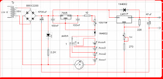
Power Supply Kamera Digital

DIGITAL CAMERA PSU AND BATTERIES CHARGER

 
This ambit was created for agenda cameras. It's accepted the agenda cameras accept ample
ability consumption. For archetype my camera Minolta E223 requires about 800 mA. In
convenance a mains ability accumulation or aerial accommodation NiMH accumulators
(batteries) can amuse this demand.
This ambit consists of two parts, charger and adapter. The transformer, rectifier arch
and absorber condensator are common. Adapter is absolutely artlessly its capital
allotment is an adjustable voltage regulator LM 317 according to accepted setting.
Output is a acceptable for camera jack plug. Voltage can be adapted in ambit 2-9 V.
In the charger ambit a 7805 anchored voltage regulator works as accepted architect
assured connected accepted during charging. This charging accepted can be adapted with
the 100 /1W potentiometer in ambit about 50-300 mA adumbrated by a baby accepted
barometer instrument. From one to four batteries can be answerable simultaneously. The
about-face charge be set according to cardinal of batteries, and charging accepted of
batteries accustomed by architect charge be adjusted. This ambit doesn't admeasurement
charging time and charging action of batteries. Manufacturers accord charging time,
usually 14-16 h. I apparent this botheration with a simply, bargain automated mains
timer. I anticipate its accurateness is sufficient.
Source   skema-amplifier.blogspot.com

25Watt Audio Amplifier Mosfet

25Watt Audio Amplifier Mosfet IRF530-IRF9530


The following is a circuit of 25Watt High Quality power amplifier Mosfet IRF530-IRF9530
from Motorola's transistors are employed in the preceding stages. The supply rails
prudentially voltage was kept at the rather low value of + and - 32V.
Skema Rangkaian 25Watt Audio Amplifier Mosfet
Note:
Q6 & Q7 must have a small U-shaped heatsink.
Q8 & Q9 must be mounted on heatsink.
Adjust R11 to set quiescent current at 100mA (best measured with an Avo-meter connected
in series to Q8 Drain) with no input signal.
A correct grounding is very important to eliminate hum and ground loops. Connect to the
same point the ground sides of R1, R4, R9, C3 to C8. Connect C11 to output ground. Then
connect separately the input and output grounds to power supply ground.
List Component

R1,R4_________47K 1/4W Resistors
R2____________4K7 1/4W Resistor
R3____________1K5 1/4W Resistor
R5__________390R 1/4W Resistor
R6__________470R 1/4W Resistor
R7___________33K 1/4W Resistor
R8__________150K 1/4W Resistor
R9___________15K 1/4W Resistor
R10__________27R 1/4W Resistor
R11_________500R 1/2W Trimmer Cermet
R12,R13,R16__10R 1/4W Resistors
R14,R15_____220R 1/4W Resistors
R17___________8R2 2W Resistor
R18____________R22 4W Resistor (wirewound)
C1___________470nF 63V Polyester Capacitor
C2___________330pF 63V Polystyrene Capacitor
C3,C5________470µF 63V Electrolytic Capacitors
C4,C6,C8,C11_100nF 63V Polyester Capacitors
C7___________100µF 25V Electrolytic Capacitor
C9____________10pF 63V Polystyrene Capacitor
C10____________1µF 63V Polyester Capacitor
Q1-Q5______BC560C 45V 100mA Low noise High gain PNP Transistors
Q6_________BD140 80V 1.5A PNP Transistor
Q7_________BD139 80V 1.5A NPN Transistor
Q8_________IRF530 100V 14A N-Channel Hexfet Transistor
Q9_________IRF9530 100V 12A P-Channel Hexfet Transistor

sumber   skema-amplifier.blogspot.com

Sunday, June 12, 2011

Mini Amplifier IC LM380

Mini Amplifier IC LM380
Based amplifier IC's offer many advantages including high efficiency, high gain, low standby current, low component count, small size and, of course, low cost. It is little wonder that audio amp IC's have replaced most discrete transistors in consumer electronic devices. While many experimenters have stayed away from these little black Mysteries, I am going to uncover some of their secrets and demonstrate how easy they are to use
Rangkaian Amplifier IC LM380

Amplifier IC LM380 comes in two flavors; LM380 and LM380-8 with output powers of 700 milli-watts and 2 watts respectively. A schematic drawing below depicts the 8th and LM380-LM380.
The LM380-8 comes in an 8-pin package and its basic circuit is virtually identical to the LM380 except for the different pin out. The LM380 comes in a 14-pin package and pins 3,4,5,10,11 and 13 are connected to ground to act as a heat sink. Experience has shown the LM380 should be soldered directly to the circuit board (no IC socket) if it is going to be operated at its full rated output of 2 watts. This IC can become quite warm and it's important to get rid of excess heat through the pins. The primary advantages of the LM380 series IC's are higher output power, very low distortion and low external parts count.
Source  skema-amplifier.blogspot.com

Game Baru Tomb Raider


Game Anyar Tomb Raider Dirilis 2012


    Download Gamenya DiSini...[]

Seri terbaru Tomb Raider akan dirilis 2012
LOS ANGELES - Pengembang game Crystal Dynamics berencana meluncurkan seri terbaru instalemen game populer Tomb Raider pada 2012 mendatang.Pengumuman itu disampaikan Crystal Dynamics pada perhelatan Electronic Entertainment Expo (E3) 2011 yang dimulai Selasa waktu setempat di Los Angeles Convention Center.
Belum diketahui apa judul yang akan disematkan pada instalemen terbaru Tomb Raider
tersebut. Namun trailer dan sejumlah cuplikan gameplay-nya sudah dipamerkan pihak
pengembang pada pameran tersebut.Pada seri terbaru ini, tokoh utama Lara Croft tampil sebagai wanita 21 tahun yang baru lulus kuliah dan haus akan petualangan. Jiwa petualangan Lara akhirnya membawa dirinya terdampar di pulau misterius dengan penghuni pulau yang membahayakan.
Menurut Head of Studio Crystal Dynamics Darrell Gallagher, seri ini menceritakan petualangan Lara Croft sebelum menjadi tokoh jagoan wanita yang dikenal para gamer seluruh dunia.
"Perjalanan tersebut akan menentukan karakter Lara di masa mendatang. Game ini
menceritakan bagaimana dia menemukan jati dirinya dan berhasil menjadi prajurit tangguh
setelah melewati petualangan tersebut," jelas Gallagher seperti dikutip Bit Tech, Rabu (8/6/2011).
Rencananya game terbaru Tomb Raider baru akan rilis pada musim gugur 2012.
(van). source   okezone.com

100 watt Amplifier for Car

100W Quad Car Amplifier


 This quad ?nal amplifier is actually intended to be used in a car, but it can naturally also be used for a variety of other medium-power applications. The TDA7375A can be successfully used in all situations in which a reasonable amount of audio power is desired and only a relatively low supply voltage is available. This IC is the successor to the TDA7374B, which forms the heart of the active loudspeaker system described earlier this year. Such a quad IC amplifier is naturally an excellent choice for this application, especially since the individual amplifiers can be connected in pairs in the bridge con?guration, which allows them to provide approximately four times as much power.The new IC can handle a peak voltage of 50 V (10 V more than the TDA7374B), but what is more important is that it is also truly intended to be used for single-ended operation. It includes all imaginable types of protection in order to avoid the premature demise of the four amplifiers, and in fact it is ideally suitable for a ‘no-nonsense’ mini surround-sound system. For more information about the TDA7375A, we refer you to its data sheet, which can be found at www.st.com. The circuit shown here has four trimpots for individually setting the output levels of the amplifiers.

In addition, all inputs have RC networks (R1/C1, etc.) to block possible RF interference. The function of R6 is to separate the grounds of the input and output stages, in order to avoid possible ground loops that might arise with the use of multiple modules. A 5-W type is used for this resistor, in order to prevent it from going up in smoke if the ground connection of the power supply comes loose. C10 decouples the internal voltage divider, which biases the internal amplifier stages to half of the supply voltage. RC network R5/C9 provides a delayed, plop-free switch-on.

C15 and C16 are local bypass capacitors for the supply voltage. The power supply ripple rejection of the TDA7375A is approximately 50 dB. If you want to use only a transformer, bridge rectifier and smoothing capacitor for the power supply, the minimum requirement is a transformer rated at 12 V / 30 VA in combination with a 10,000-µF electrolytic capacitor (remember that the maximum allowable supply voltage is 18 V). One of the few drawbacks of this quad ampli?er is that two of the channels are inverted with respect to the other two. For this reason, the polarity of each loudspeaker terminal is marked on the circuit board layout (e.g., +LS1 and –LS4) to indicate which terminal of the loudspeaker should be connected where.

Radial electrolytic capacitors rated at 3300µF/16V and having a diameter of only 12 mm are used for the output capacitors, which allows the circuit board to remain relatively compact. Our preferred type of electrolytic capacitor is a member of the Rubycon ZL series, which can handle no less than 3.4 A of ripple current. The maximum current consumption of the circuit with all four channels driven to the clipping level (with 4-? loads) is approximately 2.1 A. The TDA7375A can also be used with 2-? loads. However, in this case the internal temperature rises considerably, since the Multiwatt 15V package has a rather large thermal impedance of 1.8 ºC/W.

In the interest of the service life of the IC, it is thus a good idea to use a somewhat larger heat sink. A 4 A/T fuse has been selected in consideration of possible 2-? operation. If you limit the load to 4 ?, the fuse value can be reduced to 2 A/T. The output terminals of the ampli?ers can be found on the circuit board next to the associated electrolytic capacitors. The related ground connections for LS1 and LS2 are located next to the LS1 and LS2 terminals, but the ground connections for LS3 and LS4 are located on the left, next to the IC, since this gives the best current paths on the circuit board and the least distortion. Vertical car connectors (spade terminals) are used for the power supply connections.

Resistors:
R1-R4 = 100?
R5 = 10k?
R6 = 0?1, 5W
P1-P4 = 10 k preset
Capacitors:
C1,C3,C5,C7 = 15nF
C2,C4,C6,C8 = 220nF
C9 = 10µF 63V radial
C10 = 47µF 25V radial
C11-C14 = 3300µF 16V
C15 = 100nF
C16 = 1000µF 25V radial, max. diameter 13mm
Semiconductors:
IC1 = TDA7375A (ST)
Miscellaneous:
F1 = fuse, 4A/T (time lag), with PCB mount holder 2 fast-on (spade) terminal, male, vertical, solder type (2-pin version)
Measurement results
Supply voltage = 14.4 V
Quiescent current = 100 mA
Pmax. (0.1% THD) = 4 x 5.3 W/ 4?
Input sensitivity = (5.2 W/4 ?) 0.5 V
THD+N (B = 80 kHz, 1 kHz 1W/4 ?) = < 0.04 % Bandwidth = 28 Hz to 55 kHz
source   extremecircuit.net

50W Audio Amplifier Using TDA1562

50W Audio Amplifier Using TDA1562

The integrated output amplifier described in this article consists of little more than one integrated circuit. It is intended especially for use in motor vehicles and other battery-operated applications. Although it appears simple and hardly worth looking at, the amplifier can produce an appreciable audio power output. The circuit diagram in Figure 2 emphasizes how few external components are needed to construct a complete output amplifier.
For instance, the new device does not need compensation networks to enhance the stability. Also, because of the absence of switch-on phenomena, there is no need for a switch-on delay network. There is, of course, still a need for supply line decoupling capacitors. Capacitors C5 and C6 are required for Class-H operation, about which more in the box. The value of input capacitors C1 and C2 is relatively low, thanks to the high input impedance of the IC. Switched RC network R4-C4 at the ‘mode select’ input (pin 4) serves to switch the IC to ‘mute’ or ‘standby’.
When the supply voltage is switched on, the IC is first switched automatically to the ‘mute’ mode and to ‘on’ only after a short delay. The time constant R4-C4 is a few tenths of a second and this delay between the two states is sufficient to obviate disturbing (and annoying) switch-on phenomena. Switch S1 enables the amplifier to be switched to ‘standby' when the use of the amplifier is not needed for a period of time. When that time has elapsed, the amplifier is quickly reverted to normal operation. The current drain in the standby mode is virtually negligible at only 200µA. Resistor R3 prevents a short-circuit current ensuing when S1 is being closed at the instant C4 is being discharged.
Measurement results (at Ub=14.4 V)
Supply voltage
8–18 V
Sensitivity
760 mV r.m.s.
Input impedance
70 k?
Power output
54 W r.m.s. into 4 ? (f=1 kHz; THD+N=1%)
Harmonic distortion (THD+N)
at 1 W into 4 ?: 0.046% (1 kHz)
0.29% (20 kHz)
at 35 W into 4 ?: 0.12% (1 kHz)
0.7% (20 kHz)
Signal-to-noise ratio (with 1 W into 4 ?)
88 dBA
Power bandwidth
7.5 Hz – 185 kHz (at 25 W into 4 ?)
Quiescent current
about 135 mA (‘on’)
Resistors:
R1 = 1M?
R2 = 4k?7
R3 = 1k?
R4 = 100k?
Capacitors:
C1,C2 = 470nF
C3,C4 = 10µF 63V radial
C5,C6,C8 = 4700µF 25V radial
(18mm max. dia., raster 7.5 mm)
C7 = 100nF, raster 5 mm
Semiconductors:
D1 = high-efficiency-LED
IC1 = TDA1562Q (Philips)
Miscellaneous:
S1 = single-pole on/off switch
Four spade connectors, PCB mount Heatsink for IC1 (Rth<2.5 K/W)
sumber  extremecircuit.net

Rangkaian Infrared Cordless Headphone Amplifier

Rangkaian Infrared Cordless Headphone Amplifier

Using this low cost Project one can reproduce AUDIO from TV without disturbing anyone. It does not use any wire between TV and HEADPHONE. In place of pair of wires it uses invisible Infrared light to transmit audio signals from TV to Headphone. Without using any lens a range of up to 6 meters is possible. Range can be extended by using Lenses and Reflectors with IR sensors comprising transmitters and receivers. IR transmitter uses two-stage transistor amplifier to drive two IR leds connected in series. An audio output transformer is used (in reverse) to couple Audio output from TV to the IR transmitter.
source   skema-amplifier.blogspot.com

Saturday, June 11, 2011

Rangkaian USB Sound Card

Rangkaian USB Sound Card PCM2702

The core of this construction is 16-Bit Stereo Digital-To-Analog Convertor with USB interface PCM2702.
PCM2702 needs only few additional parts to work. The schematic is not complex. Sound card can be powered directly from USB port (jumper W1) or from external power supply (jumper W3). PCM2702 needs two power supply 3.3V (3V-3.6V) and 5V (4.5V-5.5V). I used fixed output voltage LDO TPS76733Q for 3.3V (IO2) and adjustable output voltage LDO TPS76701Q for 5V (IO3). Both LDO are produced by TI, I used this because I had it in my drawer. Any similar LDO can be used. Output voltage of IO3 should be set to little bit lower than input voltage to allow LDO good stabilization, in my case output voltage is set to 4.8V. Output voltage can be set by adjustable resistor R33. In case of low power supply, IO3 can be shorted by jumper W3. LED D3 signalizes power on.
Small ferrite beads are placed before all power pins of PCM2702 and in Vbus and GND of USB. These small beads reduce high frequency hum. I had a problem find this small SMD ferrite beads in local stores but finally I acquire few of them from old hard drive. They are not absolutely necessary, you can use zero ohm resistors instead of them.
Low-pass filter is placed in output signal path to reduce sampling frequency. An OPA2353UA dual op amp is configured as a stereo 2nd-order low-pass filter. Led diode D1 is illuminated when PCM2702 plays audio data received from the USB bus. Led diode D2 is illuminated when USB bus suspends audio data transmission to the PCM2702.


IC 4069 Alternating On-Off Switch Circuit

 
Get the circuit instead of a standard on-off switch. Switching is very gentle. If we don’t use the PCB, connect unused input pins to an appropriate logic level (’+’ or ‘-’). Unused output pins *NEED* be left open!
On the Print Circuit Board this has completed already . One step ’push’ activates the relay, another ‘push’ de-activates the relay.
IC1 (the 4069) is a regular Hex-inverter type and is constructed with MOS P-channel and N-channel
enhancement mode devices in a single monolithic structure.
Accessories List

R1 = 10K
R2 = 100K
R3 = 10K
R4 = 220 Ohm (optional)
C1 = 0.1µF, Ceramic (100nF)
C2 = 1µF/16V, Electrolytic
D1 = 1N4001
Led1 = Led, 3mm, red (optional)
Q1 = 2N4401 (see text) IC1 = 4069, CMOS, Hex Inverter (MC14069UB), or equivalent
S1 = Momentary on-switch
Ry1 = Relay )
Description of circuit.
It is going to operate on voltages from 3 to 18 volts, but most applications are in the 5-15 volts. Although the IC1 4069 contains protection circuitry against damage from ESD , use common sense when handling this device. Depending on your application you may want to use an IC-socket with IC1. It makes replacement easy if the IC ever fails. The IC is CMOS so watch for static discharge! You can use any type of 1/4 watt resistors including the metal-film type.
The type for D1 in not critical, even a 1N4148 will work. But, depending on your application I would suggest a 1N4001 as a minimum if your relay type is 0.5A or more. Any one in the 1N400x series diodes will work.
Any proper replacement for Q1 will work, including the european TUN’s. Since Q1 is just a driver to switch the relay
coil, almost any type for the transistor will do. PN100, NTE123AP, BC547, 2N3904, 2N2222, 2N4013, etc. will all work for the relays mentioned here. For heavier relays you may need to change Q1 for the appropriate type.
For C2, if you find the relay acts not fast enough, you can change it to a lower value. It is there as a spark-arrestor together with diode D1.
For the relay I used an 8 volt type with the above circuit and a 9 volt battery. Depending on your application, if the current-draw is little, you can use a cheap 5V reed-relay type. Use a 8V or 9V relay type if your supply voltage is12V. Or re-calculate resistor R3 for a higher value.
The circuit and 9V will work fine and will pull the relay between 7 and 9 volt, the only thing to watch for is the
working voltage of C2; increase that to 50V if you use a 12V supply.
The pcb was designed for an Aromat/Omron relay, 12V/5A, #HB1-DC12V. You can easily re-design the relay pads on the PCB for the relay of your choice. If you wish to use something you already have, and you don’t want to re-design the PCB, you can glue the relay up-side-down on the pcb and wire the relay contacts manually to the pcb-holes or directly to your application. Use a 2N2222 transistor for Q1 if your supply voltage is higher than 9V and/or your relay is heavy duty, or doesn’t want to pull-in for any other reason.
Again, the pcb drawing is not to scale. Use ‘page-setup’ to put the scale to 103% for a single pcb, vertically, and your scale should be correct. I use a laser printer and so I don’t know if this scale of 103% is for all printers. Tocheck, print a copy onto regular paper and see if the IC pins fit the print. If so, your copy is correct. If not,
change the scale up of down until a hardcopy fits the IC perfectly.
The Led is nice for a visual circuit indication of being ‘on’. For use with 12V supply try making make R4 about 330ohms. The LED and R4 are of course optional and can be omitted. Your application may already have some sort ofindicator and so the LED and R4 are not needed.
sumber   skema-rangkaian-elektronika.blogspot.com
Free counters!