SKEMA RANGKAIAN AMPLIFIER

MELAYANI PERBAIKAN TV DAN PERANGKAT ELEKTRONIK LAINNYA. ALAMAT JL.RAYA KARANG KEMIRI RT 01/RW 06 PURWOKERTO TELP. 082329735432

Sunday, July 3, 2011

150 Watt Amplifier

This is the cheapest 150 Watt amplifier circuit you can get,I think.Based on two Darlington power transistors TIP 142 and TIP 147 ,this circuit can deliver a blasting 150 W Rms to a 4 Ohm speaker.Enough for you to get rocked?,then try out this.TIP 147 and 142 are complementary Darlington pair transistors which can handle 5 A current and 100V ,famous for their ruggedness. Here two BC 558 transistorsQ5 and Q6 are wired as pre amplifier and TIP 142 ,TIP 147 together with TIP42  (Q1,Q2,Q3)  for driving the speaker.This circuit is designed so rugged that
this can be assembled even on a perf board or even by pin to pin soldering.The circuit can be powered from a +/-45V 5A  dual power supply.You must try this circuit.Its working great.
The preamplifier section of this circuit is based around Q4 and Q5 which forms a differential amplifier. The use of a differential amplifier in the input stage reduces noise and also provides a means for applying negative feedback. Thus overall performance of the amplifier is improved. Input signal is applied to the base of Q5 through the DC decoupling capacitor C2. Feedback voltage is applied to the base of Q4 from the junction of 0.33 ohm resistors through the 22K resistor. A complementary Class AB push-pull stage is built around the transistors Q1 and Q2 for driving the loud speaker. Diodes D1 and D2 biases the complementary pair and ensures Class AB operation. Transistor Q3 drives the push-pull pair and its base is directly coupled to the collector of Q5.
Notes.
Remember TIP 142 and 147 are Darlington pairs  .They are shown as conventional transistors in figure for ease.So don’t get confused.Even though each of them have 2 transistors ,2 resistors and 1 diode inside ,only three pins ,base emitter and collector are coming out.Rest are connected internally.So its quite OK to assume each of them as transistor for ease.
Use a well regulated and filtered power supply.Connect a 10K POT in series with the input as volume control if you need.Not shown in circuit diagram.source circuitstoday

Power Supply 6 Amper

 A  +40/-40 unregulated dual supply for powering this amplifier project is shown below.  This power supply is only enough for powering one channel and for stereo applications double the current ratings of  the transformer, diodes and fuses.


source circuitstoday
Emergency Lamp 12 volt

    Here is the circuit diagram of a very versatile emergency lamp that can be operated in two modes (flasher and dimmer). The circuit is based on the dual op-amp IC LM358.The dimmer and flasher mode can be selected by using the switch S1. In the dimmer mode the output of IC1b will be pulses whose width can be adjusted by using POT R3. Transistors T1 and T2 forms the driver stage which drives the lamp L1 according to the output of IC1b. In the flasher mode, output of IC1b will be a variable frequency pulse which can be adjusted by POT R3 to obtain 1 to 25 flashes from the lamp.
Notes.
The circuit can be assembled on a Vero board.
Use a 12V battery for powering the circuit.
A heatsink must be fitted on transistor T2.
S2 can be used as an ON/OFF switch.
F1 should be a 2A fuse.
L1 can be a 12V; 2A incandescent lamp.
IC1 must be mounted on a holder.
source Circuitstoday

Friday, July 1, 2011

30 Watts Audio amplifier Circuit
A 30 watt audio amplifier circuit using TDA2040 is shown here. TDA2040 is a Class AB monolithic integrated audio amplifier available in Pentawatt package. The IC has low harmonic distortion, low cross over distortion and has a built in circuitry for short circuit protection.more >>

20 Watt Audio Amplifier Class A
The amplifier circuit uses the basic circuitry of the 70W power amplifier, but modified for true Class-A operation - it should be pretty nice! This amp has been built by several readers, and the reports I have received have been very positive. more >>


Mini Amplifier IC LM380
Based amplifier IC's offer many advantages including high efficiency, high gain, low standby current, low component count, small size and, of course, low cost. It is little wonder that audio amp IC's have replaced most discrete transistors in consumer electronic devices. more >>

The integrated output amplifier described in this article consists of little more than one integrated circuit. It is intended especially for use in motor vehicles and other battery-operated applications.
25Watt Audio Amplifier Mosfet IRF530-IRF9530
The following is a circuit of 25Watt High Quality power amplifier Mosfet IRF530-IRF9530 from Motorola's transistors are employed in the preceding stages. The supply rails prudentially voltage was kept at the rather low value of + and - 32V.more >>

Touch Switch

 A simple touch switch circuit using CD4011 is given here. The IC CD4011 is wires as a flip flop here. The 9, 13 pins of the IC works as the set and reset contacts respectively.CMOS ICs like 4011 require requires a very low current for controlling its gates. Since the pins 9 and 13 are connected to the positive via resistors R1 and R2, the logic gates of the ICs will be in high state. When we touch through the points A, B the gates of the IC will be closed and the output becomes low. This switches ON the transistor Q1 and the relay gets activated. When we touch through the points C, D the gates again becomes high and switches the transistor OFF. This makes the relay OFF. Thus by touching through the contact points A,B and C,D the appliance connected through the relay can be switched On and OFF. source   circuitstoday.

Thursday, June 30, 2011

Intercom Circuit

 A simple intercom circuit designed based on transistors is shown here. This intercom circuit does not require a changeover switch and you can use it just like a telephone and a ringer circuit is also included.
IC1 UM66 and transistor Q1 forms the ringer section. When pushbutton switch S1 is pressed UM66 produces a musical tone. This tone is amplified by Q1 and is coupled to the collector of Q2. Condenser Mic M1 is used to pick the conversation and Q2 is used to amplify it. R2 powers the condenser Mic while C2 is the DC decoupling capacitor for the amplifier stage based on Q2. The next stage of the circuit is a transformer coupled push pull amplifier stage based on L1, Q3 and Q4. Capacitor C5 is the power supply filter while capacitor C4 couples the output of the push pull amplifier to the ear piece. source  circuitstoday.

Water level Alarm Circuit

 Here is a simple water level alarm circuit that will produce an audible alarm when the water level reaches  a preset level.The circuit can be powered of a  3V battery and is very handy to use.

The circuit is based on an astable multivibrator wired around IC1 (NE 555).The operating frequency of the astable multivibrator here will depend on capacitor C1, resistances R1,R2 and the resistance across the probes A&B.When there is no water up to the probes,they will be open and so the multivibrator will not produce oscillations and the buzzer will not beep.When there is water up to the level of probes,some current will pass through the water,the circuit will be closed to some extend,and the IC will start producing oscillations in a frequency  proportional to the value of C1,R1,R2 and the resistance of water across the probes.The buzzer will beep to indicate the presence of water up to the level of the sensing probes.source circuitstoday.com

Stereo Decoder Circuits

Dingdong Sound Generator
This is the circuit diagram of a ding dong sound generator based on two NE555 timer ICs.The circuit is designed to toggle between two adjustable frequencies to produce the ding dong sound. The first NE555 (IC1) is wires as an astable multivibrator operating at 1Hz. The frequency of the second NE555 (IC2) is modulated by the output from the first IC. MORE...>

Power Supply 120 MA
12V/120mA switch mode power supply circuit.Transformer less switch mode power supplies have become very popular these days. The circuit shown below is of a 12V/120mA output, 85 to 230V AC input transformerless switch mode power supply using LNK304 IC. Applications of a power supply based on this IC includes hand held devices, timers, small appliances, LED drivers, industrial gadgets etc.LNK304 is a low component count, efficient off-line switcher IC that can support buck, buck-boost and flyback topologies. MORE...>
 
Stereo Decoder Circuit
In FM stereo transmission left and right channels are algebraically encoded into sum (left + right) and difference (left-right) signals. This is done in order to make the mono FM receivers compatible with the stereo transmission. The mono receiver will reproduce the summed left and right channel and the listener will hear both these channels through a single loud speaker. Stereo decoder is a circuit which is used in stereo FM receivers in order to recover the left and right channel information from the composite transmission signal. This task is achieved by adding the difference signal to the summed signal to recover left channel and subtracting the difference signal from the summed signal to recover the right channel. MORE...>

Stereo Decoder Circuit

In FM stereo transmission left and right channels are algebraically encoded into sum (left + right) and difference (left-right) signals. This is done in order to make the mono FM receivers compatible with the stereo transmission. The mono receiver will reproduce the summed left and right channel and the listener will hear both these channels through a single loud speaker. Stereo decoder is a circuit which is used in stereo FM receivers in order to recover the left and right channel information from the composite transmission signal. This task is achieved by adding the difference signal to the summed signal to recover left channel and subtracting the difference signal from the summed signal to recover the right channel.
The circuit diagram of a stereo decoder using MC1310P IC from Motorola is shown below. MC1310P is an integrated stereo decoder IC chip which is available in 14 pin DIL plastic package.
Circuit description.
In the circuit composite signal if fed to the input pin (pin2) of the IC through decoupling capacitor C12. Capacitors C6 and C7 do the job of power supply filtering. Capacitor C3 plus Resistors R3 and R4 forms the RC for the ICs internal oscillator circuit. Resistor R2 plus capacitors C1 and C2 forms a loop filter. D1 is an indicator LED and R1 limits the current through it. The decoded left and right stereo outputs are available at pins 4 and 5 respectively. C10 and C11 are the DC decoupling capacitors for the left and right outputs.

Temperatur Control DC Fan

Here is a simple circuit based on two transistors that can be used to control the speed of a 12 V DC fan depending on the temperature.A thermistor (R1) is used to sense the temperature. When the temperature increases the base current of Q1 (BC 547) increases which in turn decreases the collector voltage of the same transistor. Since the collector of Q1 is coupled to the base of Q2 (BD 140), the decrease in collector voltage of Q1 forward biases the Q2 more and so do the speed of the motor. Also, the brightness of the LED will be proportional to the speed of the motor.

Circuit diagram with Parts list.

Notes.
The R1 can be a 15K @ 20°C ,N.T.C  thermistor.
The M1 can be a 12V,700mA fan motor.
The capacitor C1 must be rated 25V.
The circuit can be powered from a 12V PP3 battery or 12V DC power supply.
Assemble the circuit on a good quality PCB or common board.

Wednesday, June 29, 2011

Power Supply 10 MA - 12 volt

12V/120mA switch mode power supply circuit.
Transformer less switch mode power supplies have become very popular these days. The circuit shown below is of a 12V/120mA output, 85 to 230V AC input transformerless switch mode power supply using LNK304 IC. Applications of a power supply based on this IC includes hand held devices, timers, small appliances, LED drivers, industrial gadgets etc.LNK304 is a low component count, efficient off-line switcher IC that can support buck, buck-boost and flyback topologies. The IC has a built in auto start circuit for short circuit and open loop fault protection. Other features of LNK304 includes low temperature variation, thermal shut down,high break down voltage, good line & load regulation, high band width , wide input voltage range (85 to 230V AC) etc. In general the LNK304 has a better performance when compared to the many other discrete buck regulators.LNK304 pin configuration and typical application
The pin configuration and the typical application diagram of LNK304 are shown above. Drain (D) pin the drain connection of the built in power MOSFET. The external by pass capacitor (0.1uF) is connected to the BYPASS (BP) terminal. FEEDBACK (FB) pin controls the switching of the built in power MOSFET. A current above than 49uA delivered to this pin will inhibit the switching. The internal power MOSFETs source is connected to the SOURCE (S) pin.
12V /120 switch mode power supply circuitThe circuit diagram of a practical 12V/120mA transformerless switch mode power supply is shown above.
Resistor R1, capacitors C1 and C2, diodes D1 and D2 and inductor L1 forms the input stage. D1 and D2 forms the rectifier section while C1 and C2 are input filters. Resistor R1 which is a fusible resistor limits the inrush current, increases differential mode noise attenuation and also serves as an input safetyfuse.The next stage is the regulator stage which consists of IC LNK304, diodes D3 and D4, capacitorsC3, C4 and C5, resistors R3, R4 and R5 and inductor L2. D3 is the freewheeling diode while L2 isthe output choke. C5 is the output filter capacitor which limits the output ripple voltage to a value as low as possible. The IC LNK304 is so configured that the power supply operated in the most discontinuous mode and that’s why a fast recovery diode (UF4005) is used as the freewheeling diode (D3). UF4005 has a reverse recovery time of around 75nS and it is well enough for the given situation.The voltage drop across diodes D3 and D4 are practically same and so the voltage across C4 tracks the output voltage and this voltage is picked by the network comprising of resistors R2, R3 and is fed to the feedback pin. R2 and R3 sets the output voltage and for 12V output the voltage at the feedback pin must be 1.65V DC. The circuit attains regulation by skipping the switching cycles. When the output voltage rise, the current at the feedback pin also rises and when the current rises above the threshold value, subsequent cycles are skipped until the current at the feedback pin goes below the
threshold and thus a constant output voltage is maintained.The IC will auto restart if no cycles are skipped during a 50mS time period and this limits the maximum output power to 6% of the maximum over load power. That’s how over load protection is attained. Resistor R4 serves as a small preload which nullifies the effects of tracking error.
source: http://www.circuitstoday.com

Tuesday, June 28, 2011

Dingdong Sound Generator

This is the circuit diagram of a ding dong sound generator based on two NE555 timer ICs.The circuitis designed to toggle between two adjustable frequencies to produce the ding dong sound. The firstNE555 (IC1) is wires as an astable multivibrator operating at 1Hz. The frequency of the second NE555(IC2) is modulated by the output from the first IC. This is attained by connecting the output of first IC to the control pin (pin5) of the second IC. The tone of the sound depends on the frequency of the second IC and the changeover time depends on the frequency of the first IC.
Notes.
The circuit can be assembled on a Vero board.
Use 9V PP3 battery for powering the circuit.
POT R4 can be used to adjust the tone of the sound.
POT R2 can be used to adjust the change over time.
IC1 and IC2 must be mounted on holders.
K1 can be a 8 ohms, 1/2 watt tweeter.
source:http://www.circuitstoday.com

Monday, June 27, 2011

Zero Crossing Detektor

Zero-crossing detector is an applied form of comparator. Either of the op-amp basic comparator
circuits discussed can be employed as the zero-crossing detector provided the reference voltage Vref
is made zero. Zero-crossing detector using inverting op-amp comparator is depicted in figure. The
output voltage waveform shown in figure indicates when and in what direction an input signal vin
crosses zero volt. In some applications the input signal may be low frequency one (i.e. input may be
a slowly changing waveform). In such a case output voltage vOUT may not switch quickly from one
saturation state to the other. Because of the noise at the input terminals of the op-amp, there may
be fluctuation in output voltage between two saturation states (+ Vsat and – Vsat voltages). Thus
zero crossings may be detected for noise voltages as well as input signal vin. Both of these problems
can be overcome, if we use regenerative or positive feeding causing the output voltage vout to change
faster and eliminating the false output transitions that may be caused due to noise at the input of
the op-amp.
source:http://www.circuitstoday.com

MNC TV
TV UNO


Sunday, June 26, 2011

Astro Tv online

Rangkaian Lampu Berdenyut


Konverter Dc 12-24 volt

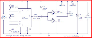
The circuit diagram of a very simple voltage doubler using NE555 timer is shown here. Here IC NE555 is wired as an astable mutivibrator operating at around 9KHz. The base of the two transistors (Q1 and Q2) is shorted and output of the astable multivibrator (pin 3) is connected to it. When the output of astable multivibrator is low, Q1 will be OFF and Q2 will be ON. The negative terminal of the capacitor C3 will be shorted to ground through T2 and it will be charged to the input supply voltage. When the output of the astable multi vibrator is high, transistor Q1 will be ON and transistor Q2 will be OFF. The capacitor C4 will be charged to the voltage across capacitor C3 plus the input supply voltage (that is double the input voltage). This is how the circuit works.
This voltage doubler circuit can deliver only up to 50mA output current and above that current limit the output voltage will be dramatically reduced. The actual output voltage will be around 19V for a 12V DC input and also the output voltage will be a bit unstable. Anyway, for low current applications this circuit is well enough.

source: http://www.circuitstoday.com

Battere Eliminator Circuit

Here is the circuit diagram of a battery eliminator circuit that can be used as a
replacement for 9V PP3 batteries. The circuit given here can be used to power any device
that operates from a 9V battery. The transformer T1 steps down the mains voltage and
bridge D1 performs the job of rectification. Capacitor C1 is a filter. IC LM317T is the
regulator here. The value of R1, R2 and R3 are so selected that the output voltage of
IC1 will be steady 9 volts.
Notes.
Assemble the circuit on a good quality PCB.
Transformer T1 can be a 230V primary, 9V secondary, 1.5A step down transformer.
If 1A Bridge is not available, then make one using four 1N 4007 diodes.
Do not connect loads that consume more than 1.5A to this circuit.
A heat sink is recommended for IC1.
source: http://www.circuitstoday.com

Saturday, June 25, 2011

Convert Cdroom to Audio cd player

    Here is the simplest scheme for converting a CD ROM drive of your computer to a Audio CD
player.The minimum requirement for the player is that, it should have a audio output and
skip button. Luckily most of the Cd ROM’s are equipped with both of these.
The CD ROM drive needs two voltages ,12V & 5V for its operation.So the main objective is
to build a suitable power supply for the CD ROM drive.The IC1 (7812) together with
associated components produce a regulated 12V DC.The IC2 (7805) together with associated
components produce a regulated 5V DC.These voltages as well as ground can be connected
to the corresponding voltage pins of the CD ROM drive using a male type CD ROM drive
power connector.The 12V can be connected to the yellow wire of connector, 5V to red wire
and GND to black wire as shown in figure1.Now the power supply is ready.
Make the circuit as shown in the circuit diagram.Power up the circuit after connecting
the power connector to the CD ROM drive. Now the power LED of the drive will glow.Insert
the audio CD.Now the music will be available at the audio output socket of the drive.It
can be heared using a headphone.The skip button of the drive can be used to play next song.
By connecting the audio output to a power amplifier you can enjoy the music in a greater
wattage.Click Here! to get the amplifier circuits suitable for this project.
Notes.
For car stereo applications you don’t need the transformer,rectifier and the 7812
regulator.12V will be available from battery.You just need to produce a 5V from it using
a 7805 based regulator. Connect the corresponding voltages to the connector as shown in
figure 1 and connect the connector to drive.Done.
The amplifier for the car audio CD player must be one operating from 12V.
Do not connect the voltages to CD ROM drive in wrong polarity.Double check the voltages
using a multimeter. Wrong polarity could easily damage the drive.
source:www.circuitstoday.com

Speaker to Microphone Converter Circuit

  This circuit is a simple approach for converting a loud speaker into a microphone. When
the sound waves fall on the diaphragm of a speaker, there will be fluctuations in the
coil and there will be a small proportional induced voltage. Usually this induced
voltage is very low in magnitude and useless. Here in the circuit the low voltage is
amplified using transistors to produce a reasonable output. The transistor Q1 is wired
in common base mode and produces the required voltage gain. The transistor Q2 is wired
as an emitter follower to produce enough current gain. The voice quality of this circuit
will not be as much as a conventional microphone but quite reasonable quality can be
obtained. To set up the circuit, keep the preset R2 at around 10 Ohms and connect the
battery. Now adjust R2 to obtain the optimum sound quality.
Notes.
Assemble the circuit on a general purpose PCB.
Power the circuit from a 9 V PP3 battery.
A 3 inch speaker can be used as K1.
All capacitors must be rated at least 15V.
An 8 Ohm speaker or head phone can be connected at the output to hear the picked sound
source: http://www.circuitstoday.com

Light to Frequency Converter Circuit

    Here is the circuit diagram of a effective light to frequency converter circuit that can
be used for variety of applications such as light intensity measurement,fun etc.
The circuit is based on TLC555, the CMOS version of famous timer IC NE 555. A photo
diode is used for sensing the light intensity.The timer IC is wired in astable mode.The
leakage current of the reverse biased photo diode is proportional to the light intensity
falling on it.This leakage current charges the capacitance C1.When the capacitor voltage
reaches 2/3 of the supply voltage the out put (pin 3) goes low.As a result the capacitor
discharges through photo diode .When the capacitor voltage reaches 1/3 the supply
voltage the out put (pin 3) of IC goes high.This cycling continues and we get a
frequency at pin 3  proportional to the light intensity falling on the photo diode.
Notes.
With the given components the frequency  varies from 1KHZ @ complete darkness to  24 Khz
@  bright sunlight.The frequency range can be changed by using different values for C1.
Use any general purpose photo diode for D1
source: http://www.circuitstoday.com

Friday, June 24, 2011

Digital To Analog Konverter

 A D/A Converter is used when the binary output from a digital system is to be converted into its equivalent analog voltage or current.The binary output will be a sequence of 1's and 0's. Thus they ma be difficult to follow. But, a D/A converter help the user to interpret easily.Basically, a D/A converter have an op-amp. It can be classified into 2 types. They are
1. Digital to Analog Converter using Binary-Weighted ResistorsA D/A converter using binary-weighted resistors is shown in the figure below. In the circuit, the op-amp is connected in the inverting mode. The op-amp can also be connected in the non-inverting mode. The circuit diagram represents a 4-digit converter. Thus, the number of binary inputs is four.Digital-to-Analog Converter Circuit - Binary-Weighted Resistors MethodWe know that, a 4-bit converter will have 24 = 16 combinations of output. Thus, a corresponding 16 outputs of analog will also be present for the binary inputs.Four switches from b0 to b3 are available to simulate the binary inputs: in practice, a 4-bit binary counter such as a 7493 can also be used.
Working
The circuit is basically working as a current to voltage converter.b0 is closedIt will be connected directly  to the +5V.Thus, voltage across R = 5V
Current through R = 5V/10kohm = 0.5mA
Current through feedback resistor, Rf = 0.5mA (Since, Input bias current, IB is negligible)
Thus, output voltage = -(1kohm)*(0.5mA) = -0.5V
b1 is closed, b0 is open
R/2 will be connected to the positive supply of the +5V.
Current through R will become twice the value of current (1mA) to flow through Rf.
Thus, output voltage also doubles.
b0 and b1 are closed
Current through Rf = 1.5mA
Output voltage = -(1kohm)*(1.5mA) = -1.5V
Thus, according to the position (ON/OFF) of the switches (bo-b3), the corresponding “binary-weighted” currents will be obtained in the input resistor. The current through Rf will be the sum of these currents. This overall current is then converted to its proportional output voltage. Naturally, the output will be maximum if the switches (b0-b3) are closedV0 = -Rf *([b0/R][b1/(R/2)][b2/(R/4)][b3/(R/8)]) – where each of the inputs b3, b2, b1, and b0 may either be HIGH (+5V) or LOW (0V).The graph with the analog outputs versus possible combinations of inputs is shown below.Digital-to-Analog Converter Circuit - Binary-Weighted Resistors Method GraphThe output is a negative going staircase waveform with 15 steps of -).5V each. In practice, due to the variations in the logic HIGH voltage levels, all the steps will not have the same size. The value of the feedback resistor Rf changes the size of the steps. Thus, a desired size for a step can be obtained by connecting the appropriate feedback resistor. The only condition to look out for is that the maximum output voltage should not exceed the saturation levels of the op-amp. Metal-film resistors are more preferred for obtaining accurate outputs.DisadvantagesIf the number of inputs (>4) or combinations (>16) is more, the binary-weighted resistors may not be readily available. This is why; R and 2R method is more preferred as it requires only two sets of precision resistance values.
2. Digital to Analog Converter with R and 2R Resistors
A D/A converter with R and 2R resistors is shown in the figure below. As in the binary-weighted resistors method, the binary inputs are simulated by the switches (b0-b3), and the output is proportional to the binary inputs. Binary inputs can be either in the HIGH (+5V) or LOW (0V) state. Let b3 be the most significant bit and thus is connected to the +5V and all the other switchs are connected to the ground.

source: http://www.circuitstoday.com
Free counters!